Superconducting nanowire avalanche photodetectors with reduced current crowding

a nanowire and photodetector technology, applied in the direction of photometry using electric radiation detectors, optical radiation measurement, instruments, etc., can solve the problems of limiting the bias current at which the device can be operated, less-than-ideal snr, and the maximum snr achieved to date remains below the theoretical value, so as to achieve lower current crowding and achieve higher achievable signal-to-noise ratios

Active Publication Date: 2017-06-29
MASSACHUSETTS INST OF TECH
View PDF3 Cites 49 Cited by
  • Summary
  • Abstract
  • Description
  • Claims
  • Application Information

AI Technical Summary

Benefits of technology

[0005]Embodiments of the present technology include SNAPs with lower current crowding and higher achievable signal-to-noise ratios (SNRs) than conventional SNAPs. An example SNAP comprises a substrate; a first nanowire disposed on the substrate and having a first straight section extending along a first direction and a first bent section electrically coupled to the first straight section; and a second nanowire disposed on the substrate and having a second straight section parallel to the first straight section and a second bent section electrically coupled to the second straight section and staggered in the first direction with respect to the first bent section.

Problems solved by technology

However, the maximum SNR achieved to date remains below the theoretical value, even in SNAPs with meandering nanowires have been developed.
This problem has also been observed in high fill-factor superconducting nanowire single photon detectors (SNSPDs) based on a single meandering nanowire.
The less-than-ideal SNR may be due to current crowding at sharp corners or non-optimal curves in the SNAP's meandering nanowires.
Areas of current crowding switch to the normal state at device bias currents less than the switching current of the nanowires composing the rest of the device and thus limit the bias current at which the device can be operated.

Method used


Image

  • Superconducting nanowire avalanche photodetectors with reduced current crowding
  • Superconducting nanowire avalanche photodetectors with reduced current crowding
  • Superconducting nanowire avalanche photodetectors with reduced current crowding

Examples


Embodiment Construction

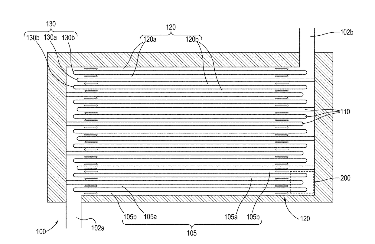
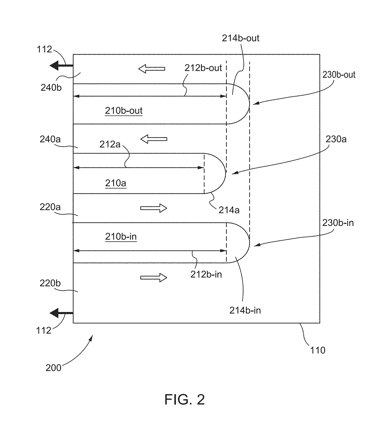
[0020]Current crowding occurs in nanowires (e.g., at bends and junctions) when the current density increases in magnitude. For example, the current density—which may be uniform in a straight section of the nanowire—may increase in magnitude near a bend or intersection in the nanowire. The increased current density acts as a weak point for the breakdown of superconductivity, either through the entry of vortices or the formation of a hotspot. Current crowding decreases the overall SNAP switching current (i.e., the current at which the SNAP witches from a superconducting state to a resistive state). For a SNAP, this decrease in switching current can reduce the SNAP's dynamic range and / or achievable signal-to-noise ratio (SNR).

[0021]Current crowding can also degrade a SNAP's sensitivity, e.g., by constraining the ability to bias the SNAP at higher switching currents. Operation at higher current is often desirable for applications where fine timing resolution is desired—the higher the bi...


PUM

PropertyMeasurementUnit
widthaaaaaaaaaa
avalanche currentaaaaaaaaaa

Abstract

Superconducting nanowire avalanche photodetectors (SNAPs) have using meandering nanowires to detect incident photons. When a superconducting nanowire absorbs a photon, it switches from a superconducting state to a resistive state, producing a change in voltage that can be measured across the nanowire. A SNAP may include multiple nanowires in order to increase the fill factor of the SNAP's active area and the SNAP's detection efficiency. But using multiple meandering nanowires to achieve high fill-factor in SNAPs can lead to current crowding at bends in the nanowires. This current crowding degrades SNAP performance by decreasing the switching current, which the current at which the nanowire transitions from a superconducting state to a resistive state. Fortunately, staggering the bends in the nanowires reduces current crowding, increasing the nanowire switching current, which in turn increases the SNAP dynamic range.

Description

GOVERNMENT SUPPORT[0001]This invention was made with Government support under Grant No. FA9550-14-1-0052 awarded by the Air Force Office of Scientific Research and under Contract No. FA8650-11-C-7105 awarded by the U.S. Air Force. The Government has certain rights in the invention.BACKGROUND[0002]A superconducting nanowire avalanche photodetectors (SNAP) comprises two or more nanowires connected in parallel between an input contact and an output contact. In operation, the nanowires are cooled below their critical temperature so that they become superconducting. While cooled, a current runs through the nanowires between the input contact and the output contact. Because the nanowires are in parallel, the current is split equally among the nanowires. Illuminating one of the nanowires with a photon creates a hotspot with increased resistance, diverting current into the other nanowire(s). This causes the current in the other nanowire(s) to exceed the critical current, which is the curren...

Claims


Application Information

Patent Timeline
Patent Type & Authority Applications(United States)
IPC IPC(8): H01L39/02G01J1/44H01L31/107
CPCH01L39/02H01L31/107G01J2001/442G01J2001/4466G01J1/44G01J1/42H10N60/84H10N60/80
Inventor SUNTER, KRISTEN ANNNAJAFI, FARAZMCCAUGHAN, ADAM NYKORUKBERGGREN, KARL KIMON
Owner MASSACHUSETTS INST OF TECH
Why Eureka
Try Eureka