Low cost hermetic micro-electronics

Active Publication Date: 2017-07-06
IBM CORP
View PDF0 Cites 3 Cited by
  • Summary
  • Abstract
  • Description
  • Claims
  • Application Information

AI Technical Summary

Benefits of technology

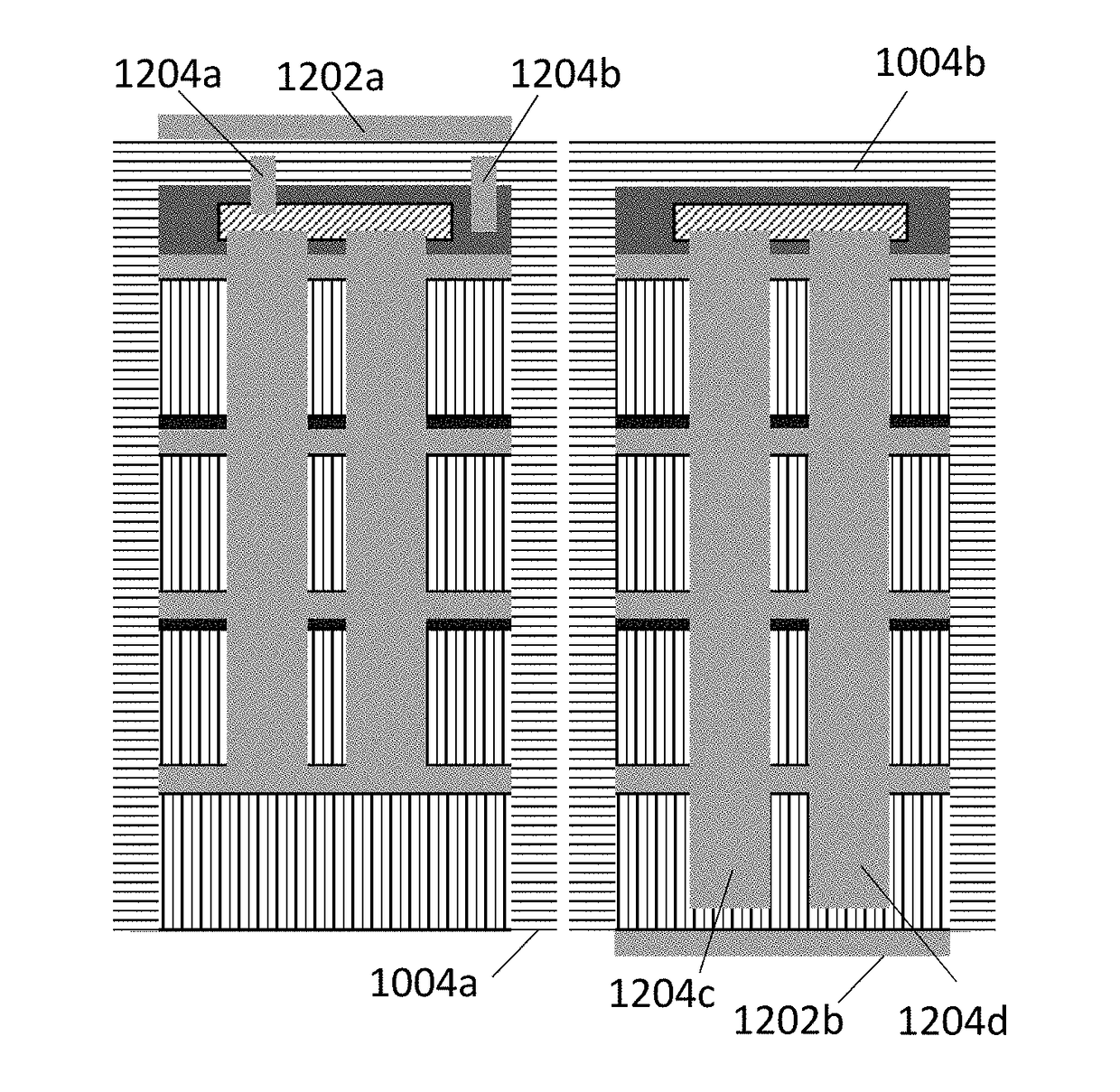
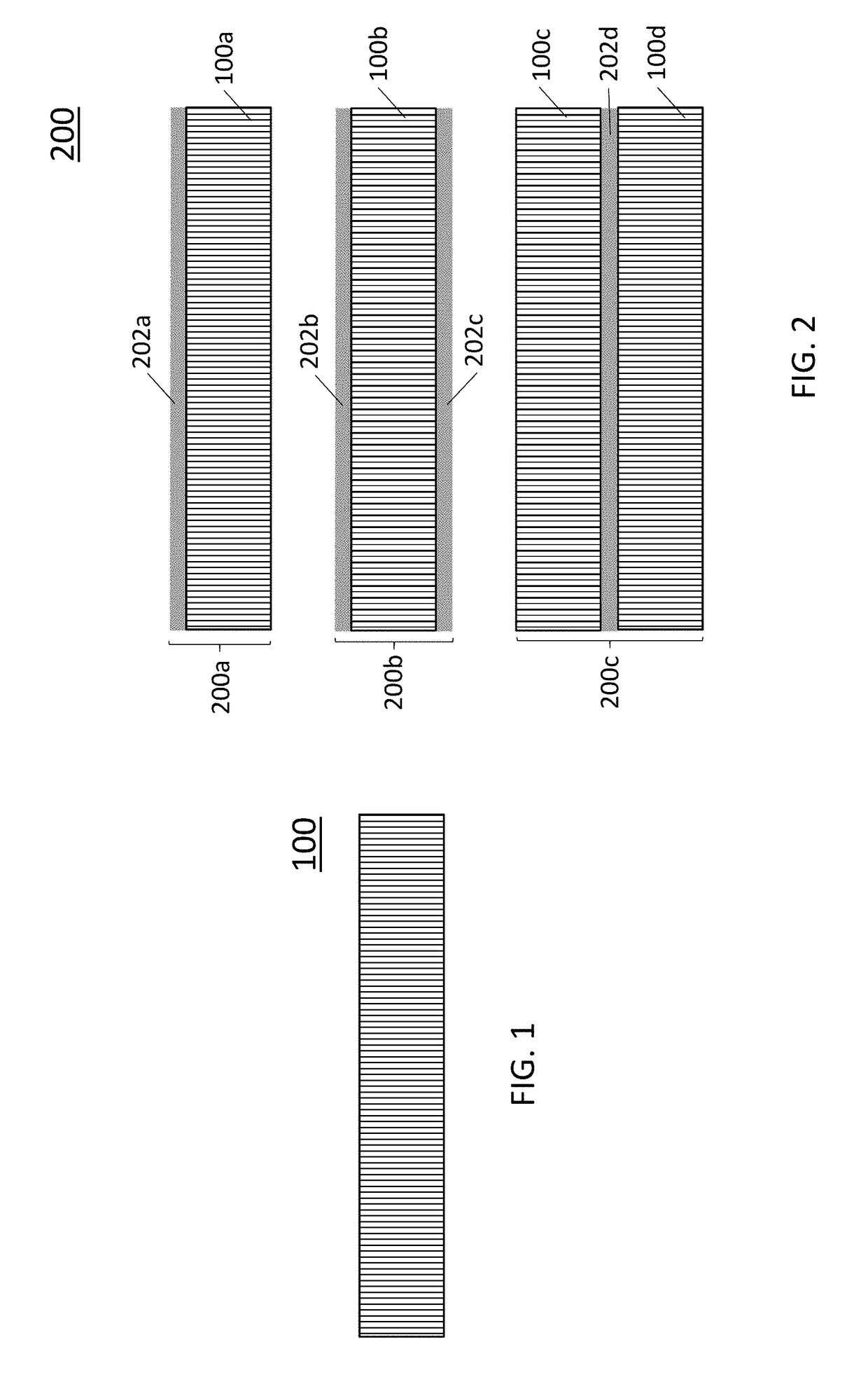
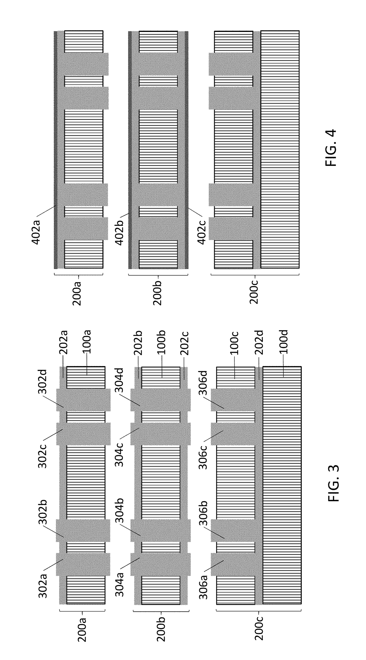
[0004]In one embodiment, a method for fabricating a hermetically sealed electronic device is disclosed. A base layer of a wafer is created using a substrate formed from ultra-thin glass or ceramic using panel or roll to roll processing. One or more layers are bonded to the base layer. Th

Problems solved by technology

However, current solutions to protect many devices are large, bulky and expensive to manufacture.
For example, pacemakers must be protected against the

Method used


Image

  • Low cost hermetic micro-electronics
  • Low cost hermetic micro-electronics
  • Low cost hermetic micro-electronics

Examples


Embodiment Construction

[0019]In this disclosure, a method is provided for use of ultra-low cost, sealed, silicon, metal, glass, polymer, composite and / or ceramic structures that can provide bio-compatibility, environmental compatibility and corrosion protection to a component, sub-component or system. Use of the disclosed methods allow for lower cost Internet of Things (IOT) sensors; health care sensors; wearable sensors; implantable sensors, systems and or tags; industrial sensors, smart tags (i.e. an electronic tag that can have information added and / or removed over time); RFID tags; and other electronic and / or optical systems. Hermetically sealed packages avoid corrosion, and are compatible with wearable and implantable solutions for human and pet use.

[0020]The disclosed methods also support high volume, small size fabrication and are environmentally friendly. The sealed electronics are isolated for bio-compatibility, electronic and / or optical functional operation, wired and / or wireless communication, ...


PUM


Abstract

A hermetically sealed electronic device and method of fabrication are provided. A base layer of a wafer is created using a substrate formed from ultra-thin glass or ceramic using panel or roll to roll processing. One or more layers are bonded to the base layer. The wafer is singulated into a plurality of electronic devices having a top surface and a plurality of sides. A hermetic sealant is applied to each electronic device to completely encase the top surface and the sides while bonding to the base layer. At least one of the layers is a metallization layer formed by metal deposition. Full metallization may be applied over the entire wafer and a pattern subsequently transferred to the full metallization by one of laser and chemical etching. The electronic device may further include at least one electronic component attached to one of the layers and encased by the hermetic sealant.

Description

BACKGROUND[0001]The present disclosure generally relates to microelectronics packaging, and more particularly relates to lost cost, high volume hermetically sealed packaging solutions for interconnection and applications such as Smart Tags, Internet of things (IOT) sensors or tags, wearable sensors, health care monitoring and implantable microelectronic devices.[0002]Many electronic devices have a need to be hermetically sealed for protection against the environment. However, current solutions to protect many devices are large, bulky and expensive to manufacture. For example, pacemakers must be protected against the fluids contacting the device so that the electronics do not corrode, thereby injuring and endangering the wearer and shortening the life of the device. Today, most pacemakers are encased in relatively large titanium boxes (e.g., around 1″ to 2″ square and about ½″ in thickness) which are welded shut and implanted within a body. The wearer's life depends upon proper funct...

Claims


Application Information

Patent Timeline
IPC IPC(8): H01L23/31H01L21/786H01L23/15
CPCH01L23/3121H01L21/786H01L23/15H01L21/486H01L23/3135H05K5/0095H05K5/0247H05K5/04
Inventor DANG, BINGKNICKERBOCKER, JOHN U.LU, MINHUANAH, JAE-WOONGPOLASTRE, ROBERT JOHN
Owner IBM CORP
Why Eureka
Try Eureka