Methods of manufacturing quantum well materials

a manufacturing method and quantum well technology, applied in the field of manufacturing quantum well materials, can solve the problems of parasitic loss in the system, low cost of methods, and inability to meet the needs of large-scale substrates,

Inactive Publication Date: 2012-08-14
GENERAL ATOMICS
View PDF12 Cites 2 Cited by
  • Summary
  • Abstract
  • Description
  • Claims
  • Application Information

AI Technical Summary

Benefits of technology

[0007]The present invention, in part, adapts the above-described methods to economical, large scale production of significantly improved quantum well materials.
[0008]Methods are disclosed for economical, large scale production of quantum well materials offering minimal or essentially no parasitic substrate loss.
[0011]Additionally, post deposition crystallization treatments are incorporated to enhance crystallization of the deposited layers and to facilitate large scale economical production.

Problems solved by technology

These methods are very costly and are not scalable to large size substrates or to cost effective mass production of large quantities of quantum well materials.
However, in thermoelectric generators, the presence of a substrate in a quantum well material becomes a parasitic loss in the system.

Method used


Image

  • Methods of manufacturing quantum well materials
  • Methods of manufacturing quantum well materials
  • Methods of manufacturing quantum well materials

Examples


Embodiment Construction

[0020]The following is a detailed description of certain embodiments of the invention presently contemplated by the inventor to be the best mode of carrying out his invention.

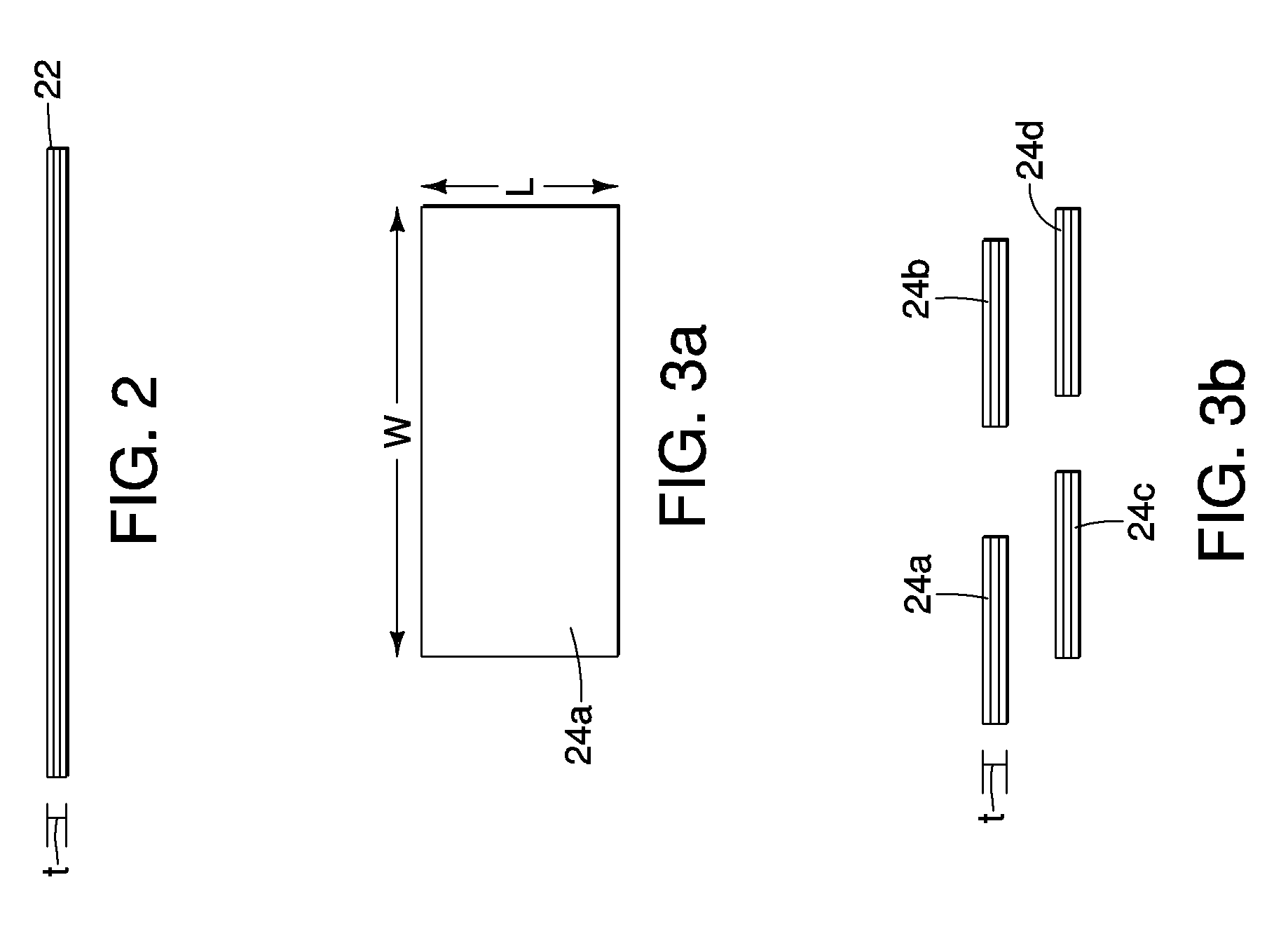
[0021]The quantum well materials produced by practice of the methods and / or processes of the invention are not here illustrated as they are generally conventional and well-known in the art. See, e.g., U.S. Pat. No. 7,038,234. In essence, quantum wells are comprised of hundreds or thousands of alternating layers of compatible semiconductor pairs, as explained above. Similarly, the equipment employed for practice of the invention is generally known in the art and for this reason is here illustrated only schematically and representatively.

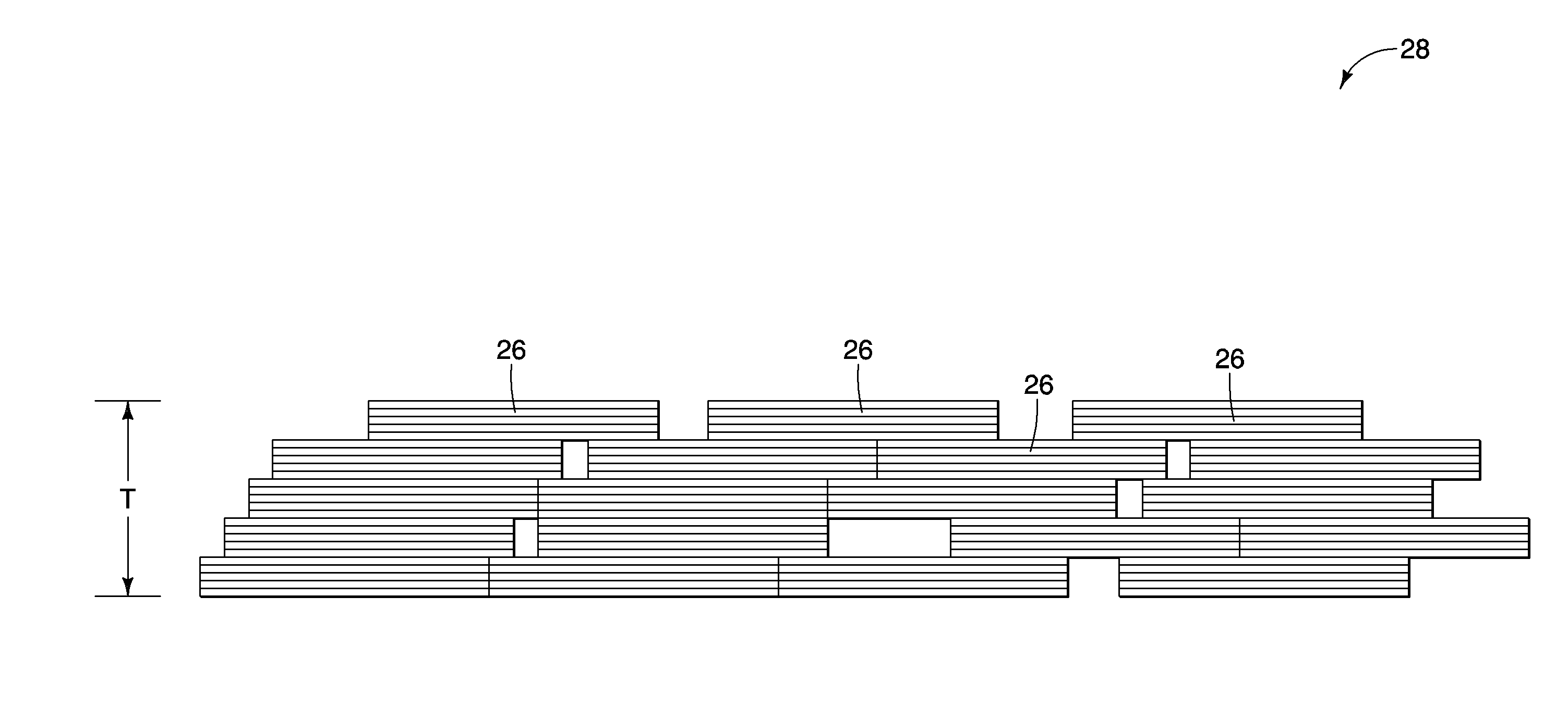
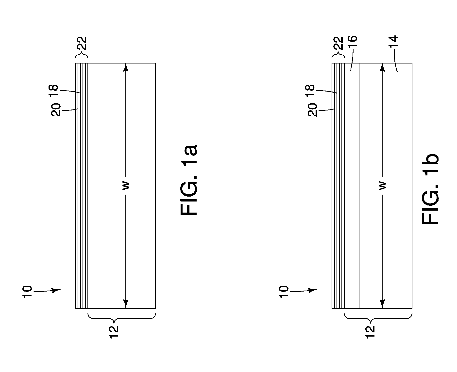
[0022]Turning now to FIGS. 1a and 1b, embodiments of methods of manufacturing a quantum well coated substrate, shown generally as 10, include providing a base layer 12. The base layer 12 is a film that is soluble in a solution, such as heated water or a solvent. The temperature a...


PUM

PropertyMeasurementUnit
thicknessaaaaaaaaaa
lengthaaaaaaaaaa
widthaaaaaaaaaa

Abstract

Processes for economical large scale commercial production of blocks of quantum well particles, platelets, or continuous sheets of material imparting minimal or essentially no parasitic substrate loss in quantum well devices such as thermo-electric generators in which the blocks are embodied involve roll to roll processing, i.e., deposition and crystallization of alternating layers of quantum well materials, on an elongate and continuous base layer of appreciable width. Blocks of quantum well materials having no attached base layer are produced on decomposable or release treated base layers.

Description

FIELD OF THE INVENTION[0001]The present invention relates to the manufacture of quantum well materials for use, for example, in thermoelectric generators and like devices.BACKGROUND[0002]Quantum well materials for use in thermoelectric generators and other similar applications are comprised of a substrate bearing hundreds or thousands of alternating layers of two semiconductor materials having the same or similar crystalline structures, one semiconductor material serving as a barrier material and the other serving as a conducting material. Typical semiconductor pairs are silicon / silicon-germanium alloy (Si / SiGe), boron / boron-carbon alloy (B / B—C), two different boron-carbon alloys such as B4C / B9C, and silicon / silicon carbide (Si / SiC).[0003]Conventional methods for depositing alternating layers of semiconductor pairs onto a substrate are thermal vapor deposition, electron beam deposition, molecular beam epitaxy and magnetron sputtering. Methods of depositing multiple layers of the pai...

Claims


Application Information

Patent Timeline
Patent Type & Authority Patents(United States)
IPC IPC(8): H01L35/34
CPCB82Y10/00H01L29/122H01L35/26H01L35/34H10N10/857H10N10/01
Inventor WOOLF, LAWRENCE D.
Owner GENERAL ATOMICS
Why Eureka
Try Eureka