Method for manufacturing a semiconductor device

a manufacturing method and semiconductor technology, applied in the direction of semiconductor devices, electrical equipment, transistors, etc., can solve the problems of reducing reliability, dielectric breakdown and short circuit, lowering film quality,

Inactive Publication Date: 2004-12-23
SEMICON ENERGY LAB CO LTD
View PDF71 Cites 16 Cited by
  • Summary
  • Abstract
  • Description
  • Claims
  • Application Information

AI Technical Summary

Benefits of technology

[0012] The present invention is characterized by heating a semiconductor film due to a heat processing method (RTA method: Rapid Thermal Anneal method) to irradiate the light emitted from a lamp light source after crystallizing the semiconductor film by laser light, thereby reducing the ridge.
[0025] Meanwhile, in the above, the substrate for forming a first semiconductor film can be a glass substrate, a quartz substrate, a metal substrate, a flexible substrate or the like. The glass substrate includes a substrate of glass such as barium boro-silicate glass and aluminum boro-silicate glass. Meanwhile, the flexible substrate refers to a film-formed substrate formed of PET, PES, PEN, acryl or the like. The manufacture of a semiconductor device is expected for weight reduction. It is desired to form a single layer or a multi-layer of barrier layers of aluminum (AlON, AlN, AlO or the like), carbon (DLC (Diamond-Like Carbon) or the like), SiN or the like on a surface or both surfaces of a flexible substrate, because durability or the like is improved.
[0026] Meanwhile, the present invention is characterized by performing a thermal crystallization method on a semiconductor film using a metal element to accelerate crystallization, and heating the semiconductor film by the RTA method after laser crystallization, there by reducing the ridge. Particularly, the ridge is conspicuously reduced by carrying out the thermal crystallization method utilizing the RTA method and further laser crystallization and thereafter heating the semiconductor film again by the RTA method. In the thermal crystallization method using a metal element, the long-time heating process with thermal anneal using a furnace anneal furnace segregates the metal element to the grain boundary, providing energetically stable state. However, if the heating time is excessively short as in the RTA method, the heating process ends before segregating the metal element to the grain boundary, making the state energetically unstable. For this reason, it can be considered that a heating process to be carried out again readily causes atom rearrangement to easily reduce the ridge.
[0042] In the invention, after laser-light crystallization of a semiconductor film, the semiconductor film is heated by a thermal processing method (RTA method: Rapid Thermal Anneal method) to irradiate the light emitted from a lamp light source, thereby reducing the ridge and obtaining a semiconductor film improved in film quality. The TFTs manufactured using such a semiconductor film improve its electric characteristic. Furthermore, The semiconductor device manufactured using the TFTs makes it possible to improve operation characteristics and reliability.

Problems solved by technology

However, the crystallization process by laser light irradiation causes to form a multiplicity of convexes (ridges) in the surface of an obtained crystalline semiconductor film, lowering film quality.
Meanwhile, the ridge at its summit is sharp and readily causes electric field concentration to possibly act as a source of current leak, eventually causing dielectric breakdown and short circuit.
In addition, the ridges in the crystalline semiconductor film surface hinder the coverage of a gate dielectric film deposited by a sputter or CVD process, reducing reliability, e.g. poor insulation.
However, if the heating time is excessively short as in the RTA method, the heating process ends before segregating the metal element to the grain boundary, making the state energetically unstable.

Method used


Image

  • Method for manufacturing a semiconductor device
  • Method for manufacturing a semiconductor device
  • Method for manufacturing a semiconductor device

Examples


embodiment 1

[0067] In order to confirm the effectiveness of the invention, the following experiment was conducted. This is explained using FIGS. 2A-2D and FIGS. 3A and 3B.

[0068] First, an underlying insulating film 11 is formed over a substrate 10. The substrate 10 is a light-transmissive glass substrate or quartz substrate. Meanwhile, the underlying insulating film 11 is provided by forming an insulating film of a silicon oxide film, silicon nitride film, silicon oxide nitride film or the like. Although the underlying film 11 herein was shown as an example using a single-layer structure, it may use a structure layered with two or more of insulating films noted above. Note that the underlying insulating film may be omitted. In this embodiment, a glass substrate was used. On the glass substrate, a silicon oxide nitride film was formed in a film thickness of 150 nm by the plasma CVD process.

[0069] Then, a semiconductor film 12 is formed on the underlying insulating film. The semiconductor film 12...

embodiment 2

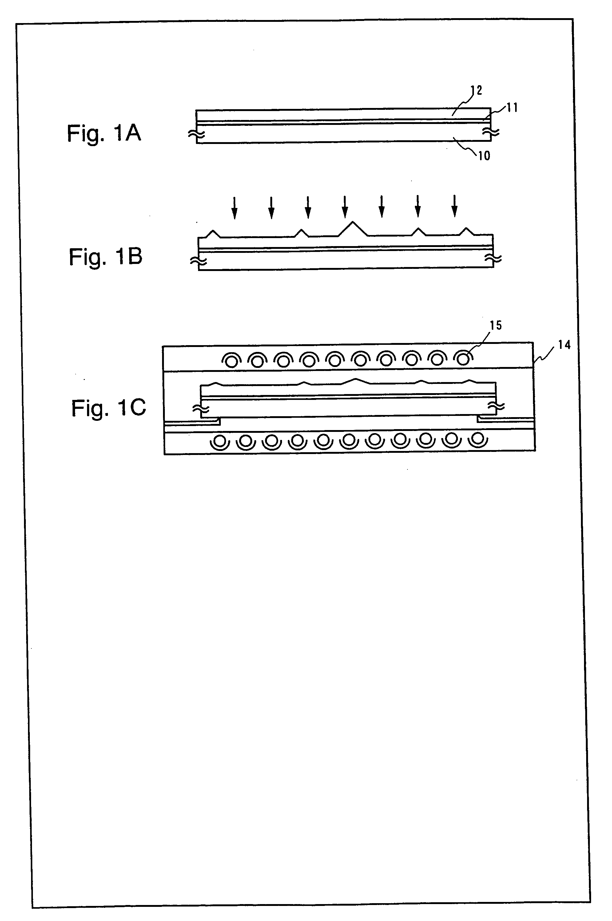
[0073] This embodiment explains a method for reducing the ridge by irradiating intense light through a different fabrication process from that of Embodiment 1, using FIGS. 1A to 1C.

[0074] First, an underlying insulating film and a semiconductor film are formed according to Embodiment 1.

[0075] Subsequently, a laser crystallization method is carried out to crystallize the semiconductor film. A laser crystallization method may be carried out after performing other known crystallizing process (thermal crystallization process, or thermal crystallization process using catalyst such as nickel). In this embodiment, a YAG-laser second harmonic wave was irradiated, which is formed in a linear shape on an irradiated plane through optical-system. This caused crystallization of the semiconductor film. However, a plurality of convexes (ridges) are formed in the semiconductor film surface. (FIG. 1B)

[0076] Subsequently, a heating process is carried out. The heating process is carried out, e.g. in a...

embodiment 3

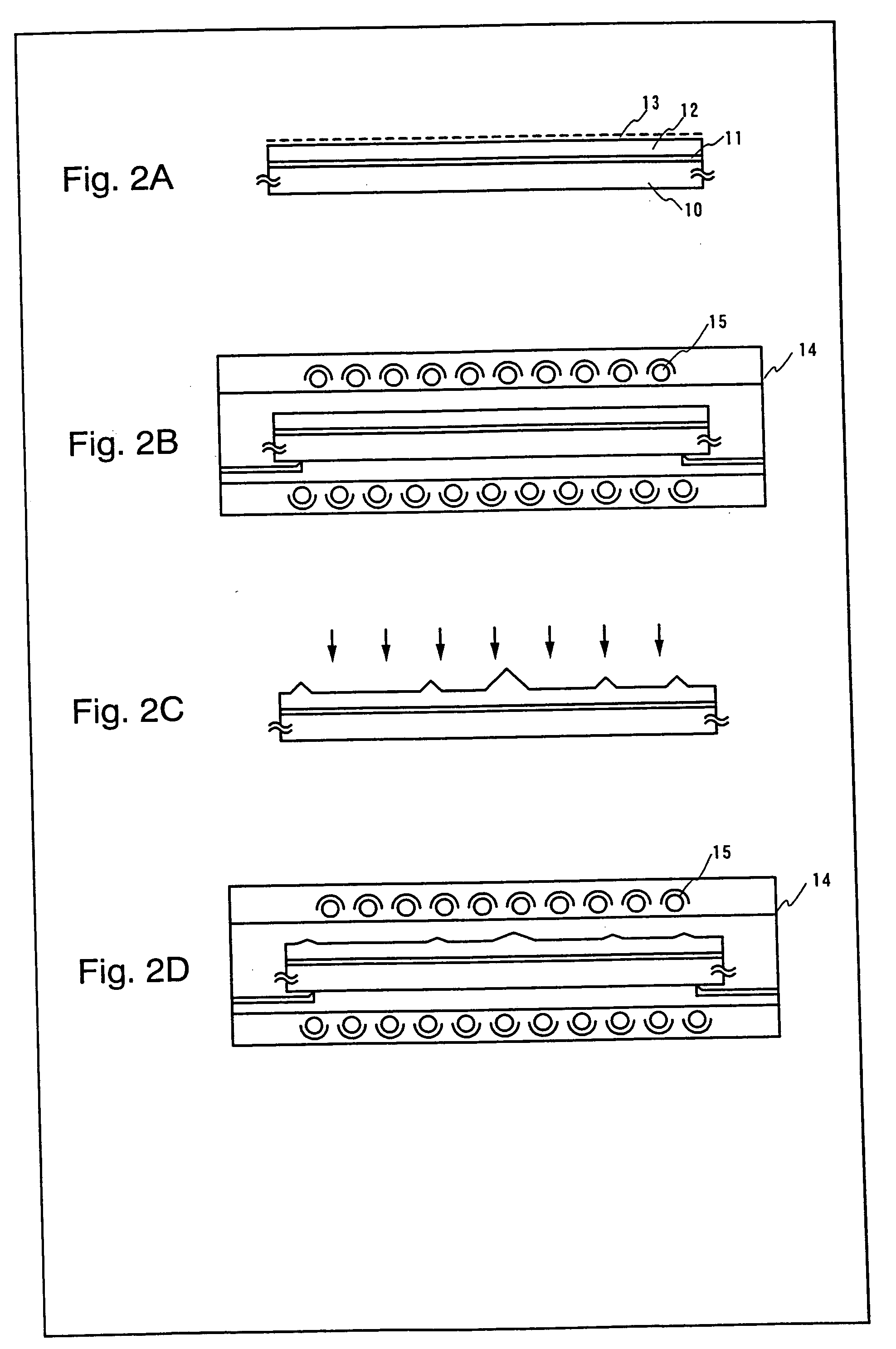
[0078] This embodiment explains a method for reducing the ridge by irradiating intense light through a different manufacturing process from those of Embodiments 1 and 2, using FIGS. 2A to 2D.

[0079] First, an underlying insulating film and a semiconductor film are formed according to Embodiment 1.

[0080] Subsequently, a laser crystallization method is carried out to crystallize the semiconductor film. A laser crystallization method may be carried out after performing other known crystallizing process (thermal crystallization process, or thermal crystallization process using catalyst such as nickel). In this embodiment, nickel 13 is introduced into the semiconductor film by a sputter process. (FIG. 2A) Then, a first heating process is performed to crystallize the semiconductor film. In this embodiment, although not shown, thermal anneal is carried out using a furnace anneal furnace. Exposure is made in an nitrogen atmosphere at a temperature of 550.degree. C. for 4 hours. Next, laser l...


PUM


Abstract

The crystallization method by laser light irradiation forms a multiplicity of convexes (ridges) in the surface of an obtained crystalline semiconductor film, deteriorating film quality. Therefore, it is a problem to provide a method for forming a ridge-reduced semiconductor film and a semiconductor device using such a semiconductor film. The present invention is characterized by heating a semiconductor film due to a heat processing method (RTA method: Rapid Thermal Anneal method) to irradiate light emitted from a lamp light source after crystallizing the semiconductor film by laser light, thereby reducing the ridge.

Description

[0001] 1. Technical Field of the Invention[0002] The present invention relates to a semiconductor device manufactured by a process to anneal a semiconductor film by the use of a laser beam (hereinafter, referred to as laser anneal), and to a method for manufacturing the same. Incidentally, the semiconductor device referred herein includes an electrooptical device, such as a liquid crystal display device and light-emitting device, and an electronic apparatus including such an electrooptical device as a part.[0003] 2. Description of the Related Art[0004] In recent years, study has been broadly made on the art to carry out laser anneal on a semiconductor film formed over an insulating substrate of glass or the like in order for crystallization or improving crystallinity. Such semiconductor films often use silicon. In the present description, the means for crystallizing a semiconductor film by using a laser beam and obtaining a crystalline semiconductor film is referred to as laser crys...

Claims


Application Information

Patent Timeline
Patent Type & Authority Applications(United States)
IPC IPC(8): H01L21/20H01L21/77H01L21/84H01L27/12H01L29/04H01L29/786
CPCH01L21/2022H01L21/2026H01L27/12H01L27/1285H01L29/78621H01L27/1277H01L29/04H01L21/02683H01L21/02488H01L21/02422H01L21/02502H01L21/0242H01L21/02672H01L21/02425H01L21/02686H01L21/02678H01L21/02532H01L21/02381H01L21/02691
Inventor YAMAZAKI, SHUNPEIOHNUMA, HIDETOTAKANO, TAMAEMITSUKI, TORU
Owner SEMICON ENERGY LAB CO LTD
Why Eureka
Try Eureka