Method for manufacturing a semiconductor device
a manufacturing method and semiconductor technology, applied in the direction of semiconductor devices, electrical equipment, transistors, etc., can solve the problems of reducing reliability, dielectric breakdown and short circuit, lowering film quality,
- Summary
- Abstract
- Description
- Claims
- Application Information
AI Technical Summary
Benefits of technology
Problems solved by technology
Method used
Image
Examples
embodiment 1
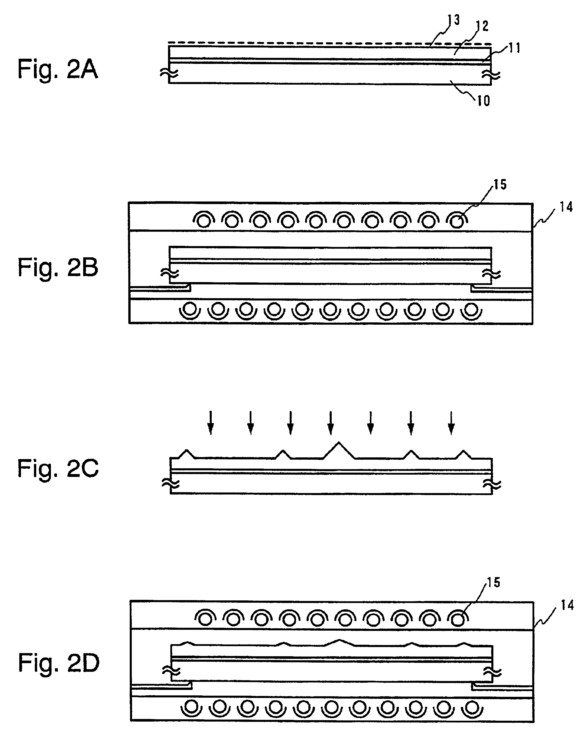
In order to confirm the effectiveness of the invention, the following experiment was conducted. This is explained using FIGS. 2A-2D and FIGS. 3A and 3B.
First, an underlying insulating film 11 is formed over a substrate 10. The substrate 10 is a light-transmissive glass substrate or quartz substrate. Meanwhile, the underlying insulating film 11 is provided by forming an insulating film of a silicon oxide film, silicon nitride film, silicon oxide nitride film or the like. Although the underlying film 11 herein was shown as an example using a single-layer structure, it may use a structure layered with two or more of insulating films noted above. Note that the underlying insulating film may be omitted. In this embodiment, a glass substrate was used. On the glass substrate, a silicon oxide nitride film was formed in a film thickness of 150 nm by the plasma CVD process.
Then, a semiconductor film 12 is formed on the underlying insulating film. The semiconductor film 12 is provided by a sem...
embodiment 2
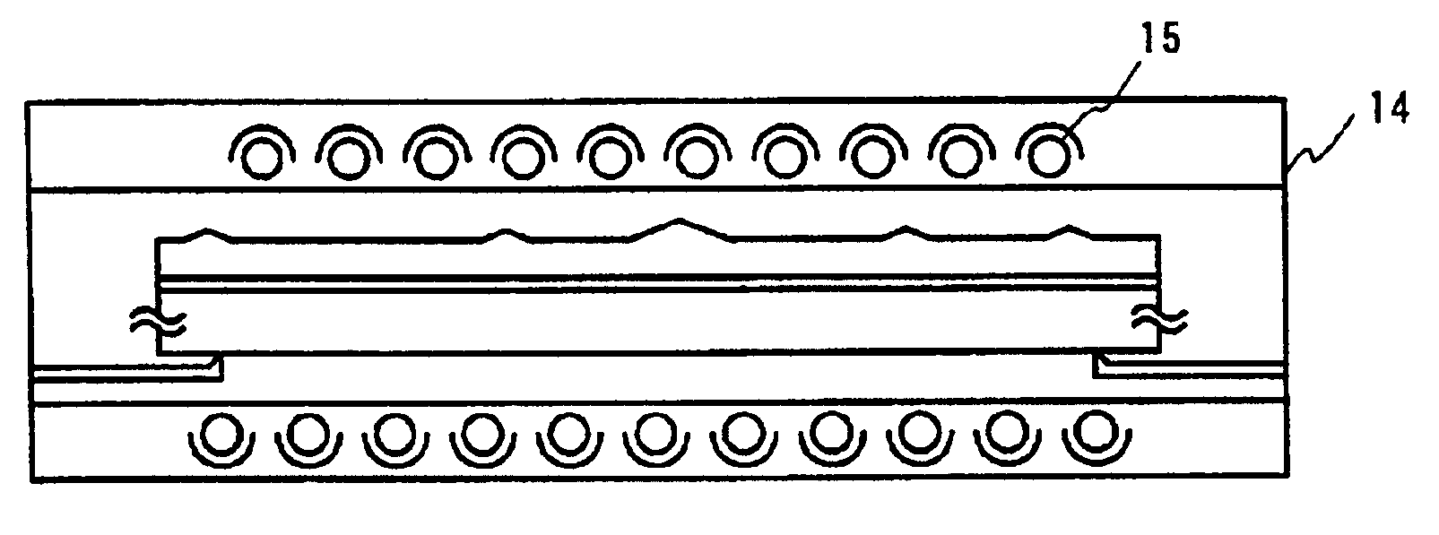
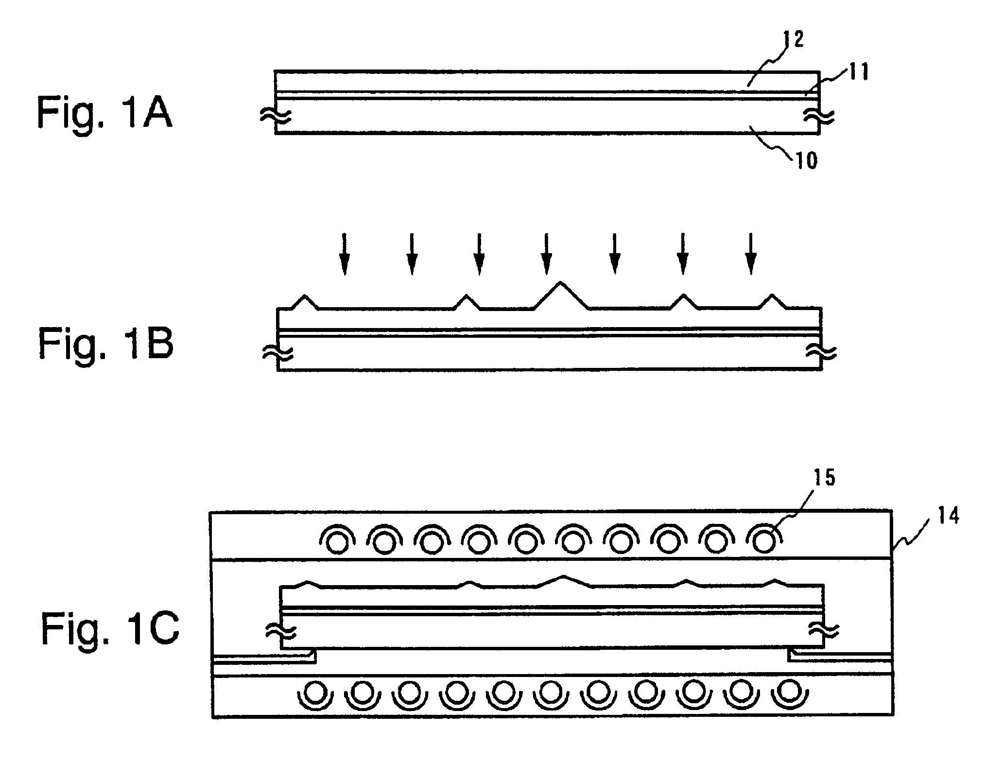
This embodiment explains a method for reducing the ridge by irradiating intense light through a different fabrication process from that of Embodiment 1, using FIGS. 1A to 1C.
First, an underlying insulating film and a semiconductor film are formed according to Embodiment 1.
Subsequently, a laser crystallization method is carried out to crystallize the semiconductor film. A laser crystallization method may be carried out after performing other known crystallizing process (thermal crystallization process, or thermal crystallization process using catalyst such as nickel). In this embodiment, a YAG-laser second harmonic wave was irradiated, which is formed in a linear shape on an irradiated plane through optical-system. This caused crystallization of the semiconductor film. However, a plurality of convexes (ridges) are formed in the semiconductor film surface. (FIG. 1B)
Subsequently, a heating process is carried out. The heating process is carried out, e.g. in a nitrogen atmosphere by turn...
embodiment 3
This embodiment explains a method for reducing the ridge by irradiating intense light through a different manufacturing process from those of Embodiments 1 and 2, using FIGS. 2A to 2D.
First, an underlying insulating film and a semiconductor film are formed according to Embodiment 1.
Subsequently, a laser crystallization method is carried out to crystallize the semiconductor film. A laser crystallization method may be carried out after performing other known crystallizing process (thermal crystallization process, or thermal crystallization process using catalyst such as nickel). In this embodiment, nickel 13 is introduced into the semiconductor film by a sputter process. (FIG. 2A) Then, a first heating process is performed to crystallize the semiconductor film. In this embodiment, although not shown, thermal anneal is carried out using a furnace anneal furnace. Exposure is made in an nitrogen atmosphere at a temperature of 550.degree. C. for 4 hours. Next, laser light is irradiated to...
PUM
 Abstract
Description
Claims
Application Information


