

Solid-state imaging element and driving method therefor, and electronic apparatus
a driving method and imaging element technology, applied in the direction of picture signal generators, television systems, radioation controlled devices, etc., can solve the problems of increasing the size of the casing, mounting costs, and difficulty in saying that the current state af speed is sufficient,
- Summary
- Abstract
- Description
- Claims
- Application Information
AI Technical Summary
Benefits of technology
Problems solved by technology
Method used
Image

Examples
first embodiment
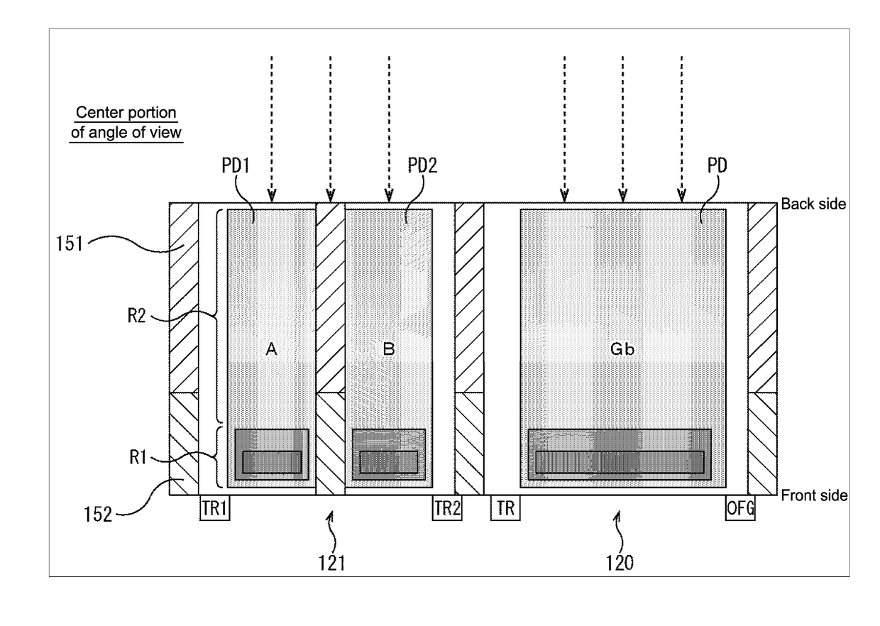
[0066]First, with reference to FIGS. 7 and 8, the first pupil correction method as the first embodiment will be described. FIG. 7 shows a sectional view of the normal pixel 120 (Gb-pixel) and the phase-difference pixel 121 in the center portion of the angle of view shown in FIG. 5. FIG. 8 shows a sectional view of the normal pixel 120 (Gb-pixel) and the phase-difference pixel 121 in the peripheral portion of the angle of view shown in FIG. 6.
[0067]As shown in FIG. 7, in the first pupil correction method, the photodiode (PD1) in the phase-difference pixel 121A is formed of a first region R1 serving as a charge accumulation main part and a second region R2 that performs photoelectric conversion and contributes to charge transfer to the main part. Furthermore, the photodiode (PD2) in the phase-difference pixel 121B is also formed of the first region R1 and the second region R2. Note that, in each of the photodiodes (PD1, PD2), the impurity concentration is represented by gradation and ...
second embodiment
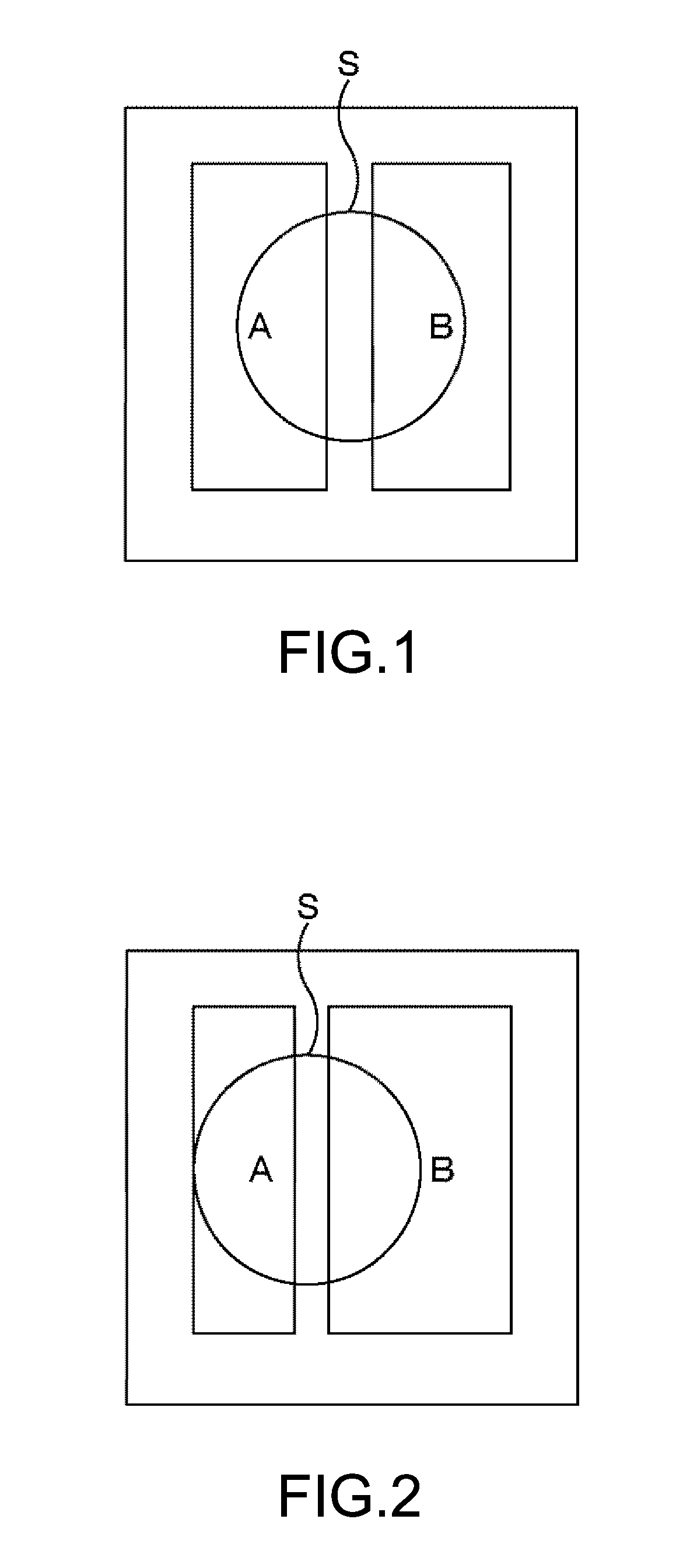
[0072]Next, with reference to FIGS. 9 and 10, the second pupil correction method as a second embodiment will be described. FIG. 9 shows a plane view of the normal pixel 120 (Gb-pixel) and the phase-difference pixel 121 in the center portion of the angle of view shown in FIG. 5. FIG. 10 shows a plane view of the normal pixel 120 (Gb-pixel) and the phase-difference pixel 121 in the peripheral portion of the angle of view shown in FIG. 6.
[0073]As shown in FIG. 9, in the second pupil correction method, as in the first pupil correction method, the photodiode (PD1) in the phase-difference pixel 121A is formed of a first region R1 serving as a charge accumulation main part and a second region R2 that performs photoelectric conversion and contributes to charge transfer to the main part. Furthermore, the photodiode (PD2) in the phase-difference pixel 121B is also formed of the first region R1 and the second region R2. Note that, in FIGS. 9 and 10, the impurity concentration in the photodiode...
PUM
 Abstract
Description
Claims
Application Information