

A method for forming a virtual germanium substrate using a laser
a laser and germanium substrate technology, applied in the direction of manufacturing tools, sustainable manufacturing/processing, final product manufacturing, etc., can solve problems such as thread dislocation defects, achieve high efficiency, avoid cvd or mbe steps, and reduce the concentration of defects
- Summary
- Abstract
- Description
- Claims
- Application Information
AI Technical Summary
Benefits of technology
Problems solved by technology
Method used
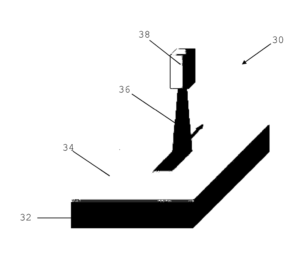
Image

Examples
Embodiment Construction
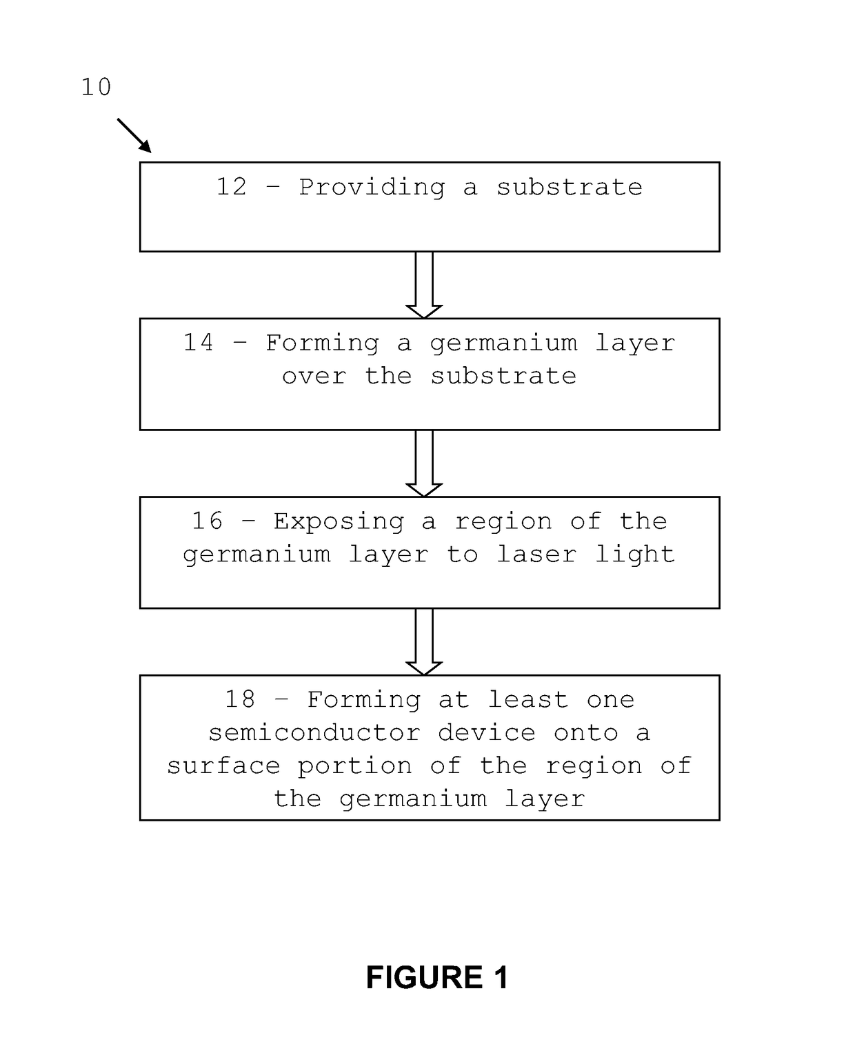
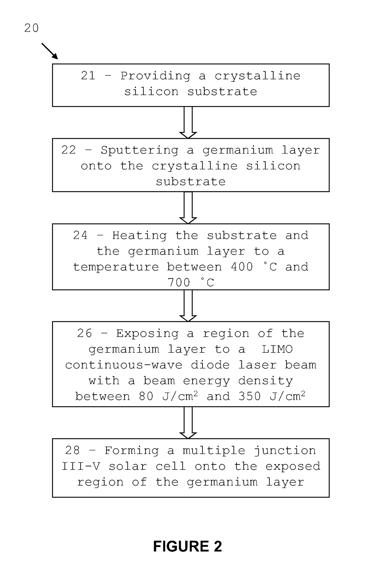
[0040]Embodiments of the present invention relate to a method of manufacturing a semiconductor device using a germanium layer. The method comprises a step of forming the germanium layer and a step of exposing a region of the germanium layer to laser light. The exposure to laser light allows reducing the concentration of defects in the germanium layer. After the exposure, the quality of the germanium layer is such that III-V semiconductor materials can be grown onto the germanium layer to form a solar cell or a light emitting diode. During the exposure of the germanium layer to laser light the concentration of defects, in particular threading dislocation defects, is reduced so that the crystalline properties of the surface portion of the germanium layer, where the semiconductor device is formed, are improved.
[0041]Epitaxial germanium layers are generally used for the growth of III-V based high efficiency solar cells. They provide a small lattice mismatch (0.08%) and almost no thermal...
PUM
| Property | Measurement | Unit |
|---|---|---|
| Temperature | aaaaa | aaaaa |
| Temperature | aaaaa | aaaaa |
| Efficiency | aaaaa | aaaaa |
Abstract
Description
Claims
Application Information