This helps you quickly interpret patents by identifying the three key elements:
Problems solved by technology
Method used
Benefits of technology
Benefits of technology
This patent text aims to provide an improved imaging device that can capture images of moving objects without distortion and retain data for a long time. The device has a simple circuit configuration and operates through a simple procedure, making it easy to manufacture at low cost. Additionally, it has high efficiency in transferring charge corresponding to imaging data, high light sensitivity, and high resolution. The device is small-sized and suitable for high-speed operation.
Problems solved by technology
Accordingly, a circuit configuration and an operating method of an imaging device operating with the global shutter method are more complicated than those of an imaging device operating with a rolling shutter method.
To increase the efficiency of transferring charge corresponding to imaging data, the transfer gate preferably overlaps a gate electrode of a transfer transistor or the like; however, this structure makes the process complicated, compared to a structure where the transfer gate does not overlap such a gate electrode.
Method used
Image
Click on the blue label to locate the original text in one second.
Reading with bidirectional positioning of images and text.
Examples
embodiment 1
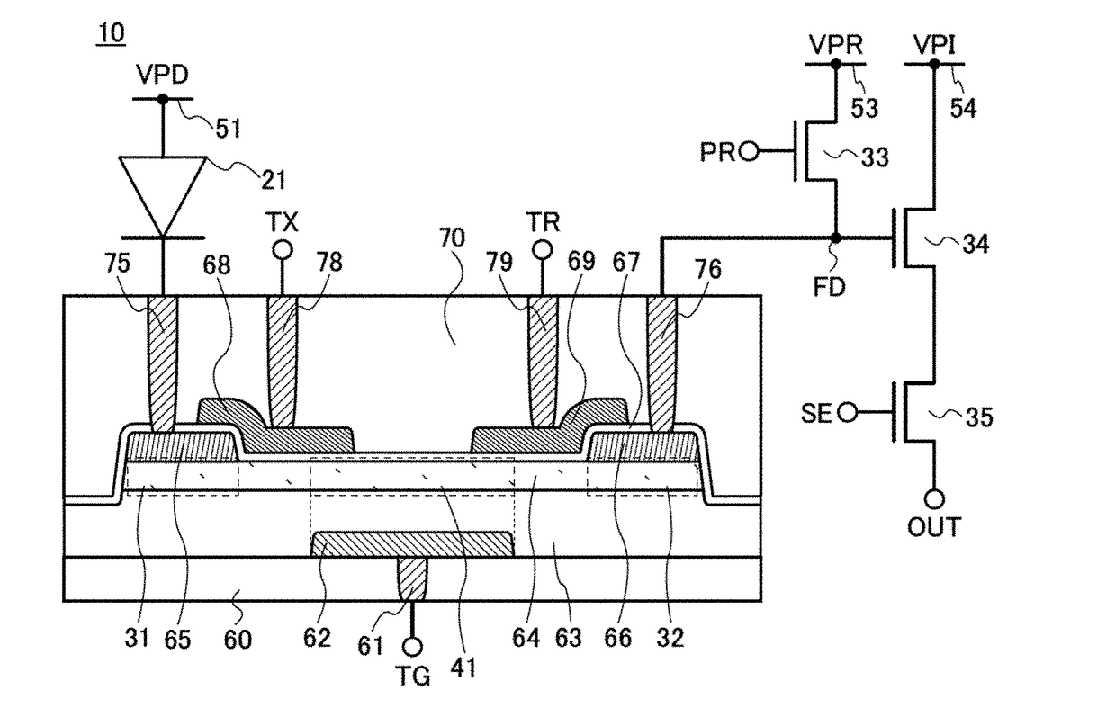
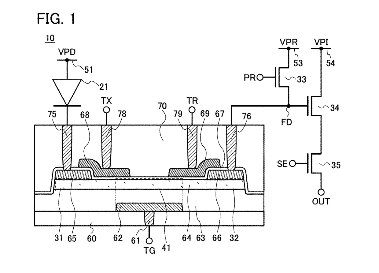
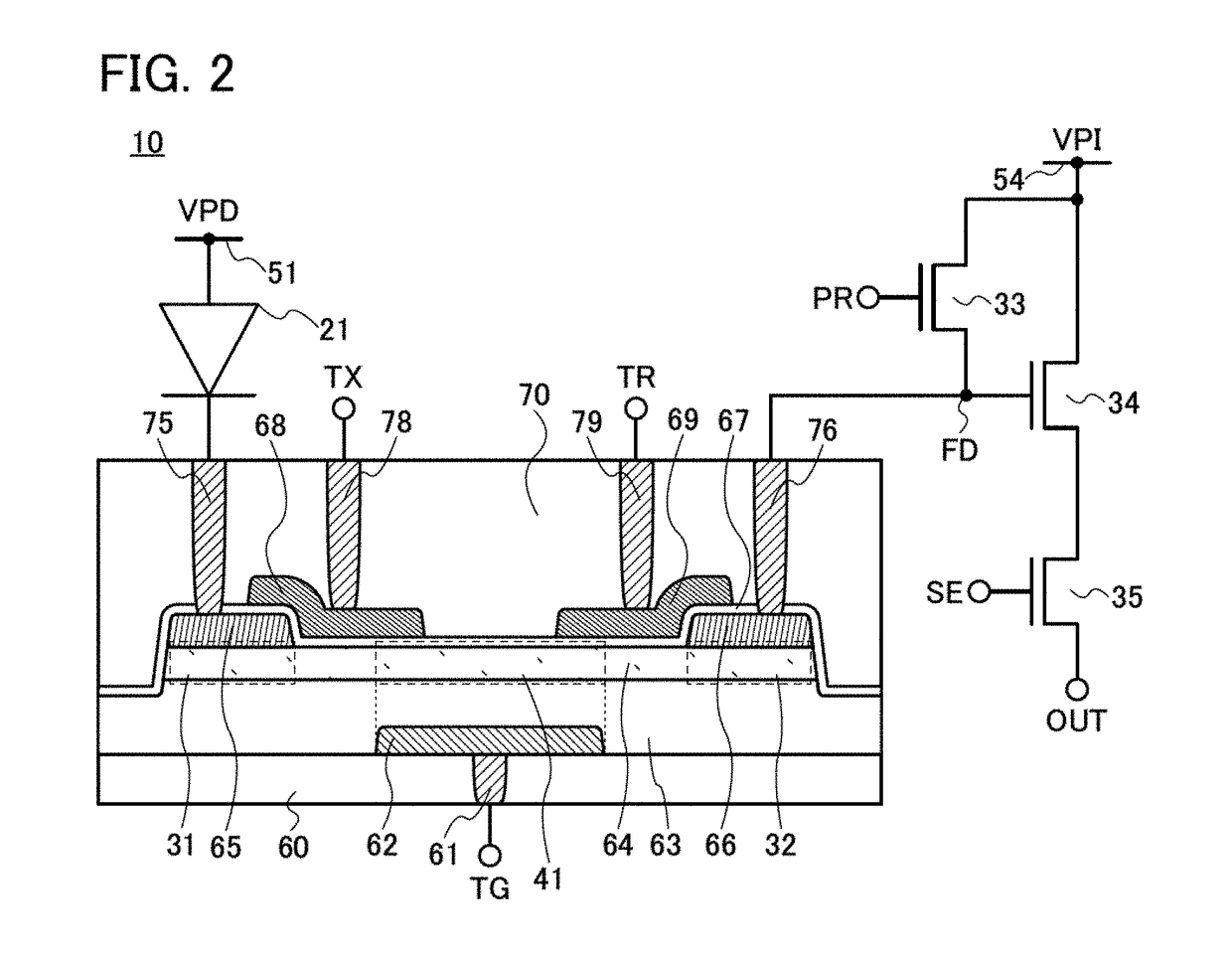
[0080]In this embodiment, an imaging device that is one embodiment of the present invention will be described with reference to drawings.
[0081]FIG. 1 illustrates a cross-sectional view and a circuit diagram that show a structure example of a pixel 10 included in an imaging device of one embodiment of the present invention. Although FIG. 1 and the like show an example using n-channel transistors, one embodiment of the present invention is not limited to this, and some transistors may be replaced with p-channel transistors.
[0082]The pixel 10 includes a conductor 62 in contact with an insulator 60; an insulator 63 in contact with the conductor 62; a semiconductor 64 in contact with the insulator 63; a conductor 65 and a conductor 66 in contact with the semiconductor 64; an insulator 67 in contact with the insulator 63, the semiconductor 64, and the conductors 65 and 66; a conductor 68 and a conductor 69 in contact with the insulator 67; and an insulator 70 in contact with the insulator...
embodiment 2
[0227]In this embodiment, an OS transistor that can be used in one embodiment of the present invention will be described with reference to drawings. In the drawings in this embodiment, some components are enlarged, reduced in size, or omitted for easy understanding.
[0228]FIGS. 22A to 22C are a top view and cross-sectional views of a transistor 301 of one embodiment of the present invention. FIG. 22A is the top view. FIG. 22B shows a cross section along the dashed-dotted line X1-X2 in FIG. 22A. FIG. 22C shows a cross section along the dashed-dotted line Y1-Y2 in FIG. 22A.
[0229]In the drawings explained in this embodiment, the direction of the dashed-dotted line X1-X2 is referred to as channel length direction, and the direction of the dashed-dotted line Y1-Y2 is referred to as channel width direction.
[0230]The transistor 301 includes a conductor 320 in contact with the substrate 310, an insulator 330 in contact with the substrate 310 and the conductor 320, an oxide semiconductor 340 ...
embodiment 3
[0274]In this embodiment, components of the transistors shown in Embodiment 2 will be described in detail.
[0275]As the substrate 310, a glass substrate, a quartz substrate, a semiconductor substrate, a ceramic substrate, a metal substrate with an insulated surface, or the like can be used. Other examples are a silicon substrate provided with a transistor and / or a photodiode; and a silicon substrate over which an insulator, a wiring, a conductor functioning as a contact plug, and the like are provided together with a transistor and / or a photodiode. When a p-channel transistor is formed on a silicon substrate, a silicon substrate with n−-type conductivity is preferably used. Alternatively, an SOI substrate including an n−-type or i-type silicon layer may be used. Moreover, when a p-channel transistor is formed on a silicon substrate, a surface of the silicon substrate where the transistor is formed preferably has a (110) plane orientation, in which case the mobility can be increased.
[...
PUM
Abstract
An object is to provide an imaging device with high efficiency of transferring charge corresponding to imaging data. The imaging device includes first to fifth conductors, first and second insulators, an oxidesemiconductor, a photoelectric conversion element, and a transistor. The first conductor is in contact with a bottom surface and a side surface of the first insulator. The first insulator is in contact with a bottom surface of the oxidesemiconductor. The oxidesemiconductor is in contact with bottom surfaces of the second and third conductors and the second insulator. Each of the second and third conductors is in contact with the bottom surface and a side surface of the second insulator. The second insulator is in contact with bottom surfaces of the fourth and fifth conductors. The first conductor has regions overlapped by the fourth and fifth conductors. The second conductor has a region overlapped by the fourth conductor. The third conductor has a region overlapped by the fifth conductor. The second conductor is electrically connected to one electrode of the photoelectric conversion element. The third conductor is electrically connected to a gate of the transistor.
Description
BACKGROUND OF THE INVENTION[0001]1. Field of the Invention[0002]One embodiment of the present invention relates to an imaging device.[0003]Note that one embodiment of the present invention is not limited to the above technical field. The technical field of one embodiment of the invention disclosed in this specification and the like relates to an object, a method, or a manufacturing method. Furthermore, one embodiment of the present invention relates to a process, a machine, manufacture, or a composition of matter. Specific examples of the technical field of one embodiment of the present invention disclosed in this specification include a semiconductor device, a display device, a liquid crystaldisplay device, a light-emitting device, a lighting device, a power storage device, a memory device, an imaging device, a method for operating any of them, and a method for manufacturing any of them.[0004]In this specification and the like, a semiconductor device generally means a device that ...
Claims
Application Information
Patent Timeline
Application Date:The date an application was filed.
Publication Date:The date a patent or application was officially published.
First Publication Date:The earliest publication date of a patent with the same application number.
Issue Date:Publication date of the patent grant document.
PCT Entry Date:The Entry date of PCT National Phase.
Estimated Expiry Date:The statutory expiry date of a patent right according to the Patent Law, and it is the longest term of protection that the patent right can achieve without the termination of the patent right due to other reasons(Term extension factor has been taken into account ).
Invalid Date:Actual expiry date is based on effective date or publication date of legal transaction data of invalid patent.

