Semiconductor quantum dot device and method for forming a scalable linear array of quantum dots

a quantum dot and semiconductor technology, applied in the field of quantum computing architectures, can solve the problems of difficult fabrication of reliable and scalable si-based quantum dots, difficult reproducible properties of quantum dots, and difficult for this trend to continue much longer

Active Publication Date: 2017-11-02
THE TRUSTEES FOR PRINCETON UNIV
View PDF1 Cites 23 Cited by
  • Summary
  • Abstract
  • Description
  • Claims
  • Application Information

AI Technical Summary

Problems solved by technology

However, as the size of transistors approaches the size of a single atom, the laws of quantum physics play an increasingly dominant role in computer architectures, making it difficult for this trend to continue much longer.
However, the fabrication of reliable and scalable Si-based quantum dots has proved challenging.
The large effective mass of electrons in Si, along with the typically lower mobilities of Si two-dimensional (“2D”) electron gases, makes the fabrication of tightly confined, few-electron, quantum dots with reproducible properties difficult.
However, there are major drawbacks to depletion mode devices with respect to control of the confinement potential and scaling.
This inability to control the electron wavefunction has led to a large variety of depletion mode gate designs, most of which do not provide a straightforward path for scaling to tens or hundreds of quantum dots.
However, depletion mode devices have very limited control over the confinement potential.
Because of such a situation, neighboring gates usually have a similar effect on the dot's tunnel couplings and electrochemical potential, and often it's not possible in depletion mode devices to tune the tunnel couplings and electrochemical potential to the desired values without going to such extreme voltages that dielectric breakdown occurs in the device.
This can make it unclear how to take existing gate patterns and extend (e.g., scale) them to tens or hundreds of quantum dots.

Method used


Image

  • Semiconductor quantum dot device and method for forming a scalable linear array of quantum dots
  • Semiconductor quantum dot device and method for forming a scalable linear array of quantum dots
  • Semiconductor quantum dot device and method for forming a scalable linear array of quantum dots

Examples


Embodiment Construction

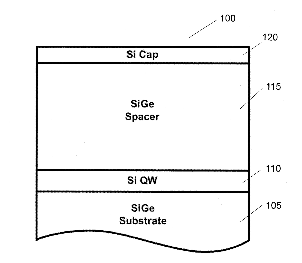
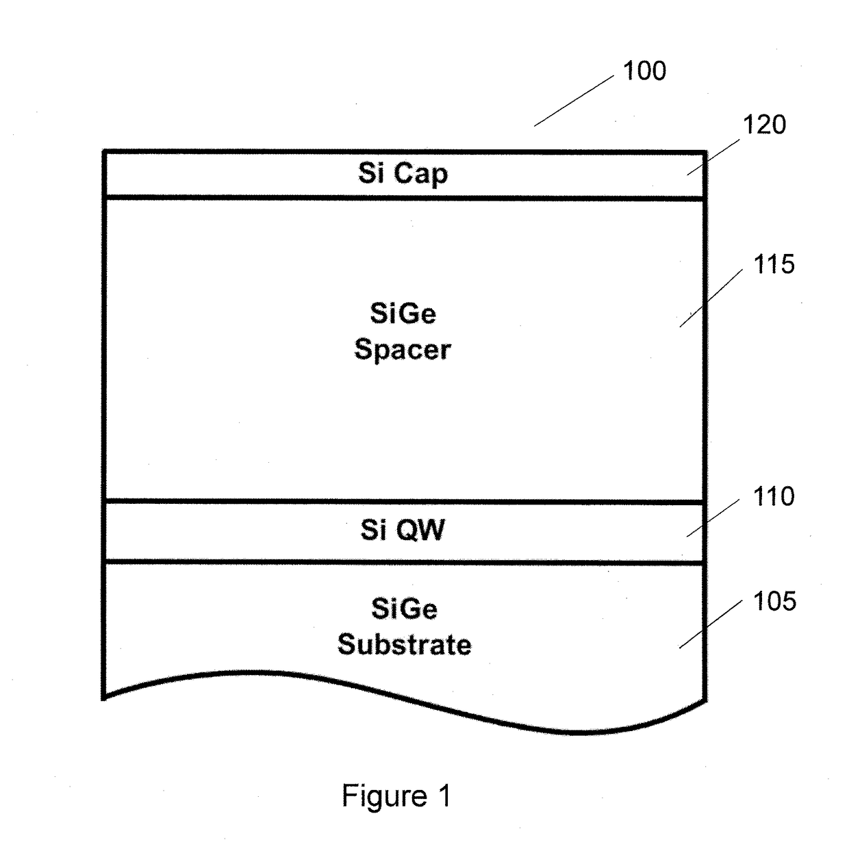
[0011]To that end, in order to overcome at least some of the deficiencies described herein above, an exemplary quantum dot device can be provided, which can include, for example, at least three conductive layers and at least two insulating layers electrically which insulate the conductive layers from one another. One of the conductive layers can be composed of a different material than the other two of the conductive layers. The conductive layers can include or be composed of (i) aluminum, (ii) gold, (iii) copper and / or (iv) polysilicon. As an alternative, the conductive layers can be composed at least partially of (i) aluminum, (ii) gold, (iii) copper and / or (iv) polysilicon. The insulating layers can be composed of (i) silicon oxide, (ii) silicon nitride or (iii) aluminum oxide.

[0012]In some exemplary embodiments of the present disclosure, the conductive layers can be composed of a metallic material having a purity rate of over 90% (e.g., 99.9%). Each of the conductive layers can ...


PUM


Abstract

An exemplary quantum dot device can be provided, which can include, for example, at least three conductive layers and at least two insulating layers electrically insulating the at least three conductive layers from one another. For example, one of the conductive layers can be composed of a different material than the other two of the conductive layers. The conductive layers can be composed of (i) aluminum, (ii) gold, (iii) copper or (iv) polysilicon, and / or the at least three conductive layers can be composed at least partially of (i) aluminum, (ii) gold, (iii) copper or (iv) polysilicon. The insulating layers can be composed of (i) silicon oxide, (ii) silicon nitride and / or (iii) aluminum oxide.

Description

CROSS-REFERENCE TO RELATED APPLICATION(S)[0001]This application relates to and claims priority from U.S. Patent Application No. 62 / 328,691, filed on Apr. 28, 2016, the entire disclosure of which is incorporated herein by reference.STATEMENT REGARDING FEDERALLY SPONSORED RESEARCH[0002]This invention was made with government support under Grant No. W911NF-15-0149 awarded by the U.S. Army, Army Research Office. The government has certain rights in the invention.FIELD OF THE DISCLOSURE[0003]The present disclosure relates generally to quantum computing architectures, and more specifically, to exemplary embodiments of an exemplary semiconductor quantum dot device and a method for forming a scalable linear array of quantum dots.BACKGROUND INFORMATION[0004]The density of transistors in integrated circuits has been following Moore's law since its conception. (See, e.g., Reference 5). However, as the size of transistors approaches the size of a single atom, the laws of quantum physics play an...

Claims


Application Information

Patent Timeline
Patent Type & Authority Applications(United States)
IPC IPC(8): H01L29/778H01L29/205H01L29/15H01L29/165H01L29/45
CPCH01L29/7783H01L29/152H01L29/452H01L29/205H01L29/456H01L29/165H01L29/7782H01L29/423H01L29/7613H01L29/0692H01L29/66977H01L31/035236H01L31/035209H01L31/035218Y02E10/50
Inventor PETTA, JASONZAJAC, DAVIDHAZARD, THOMAS
Owner THE TRUSTEES FOR PRINCETON UNIV
Why Eureka
Try Eureka