Heating chamber and semiconductor processing apparatus

a technology of semiconductor processing and heating chamber, which is applied in the direction of heating apparatus, lighting and heating apparatus, furnaces, etc., can solve the problems of limiting the capacity of the whole pvd device, the number of substrates that can be processed per unit time is relatively small, and the process is non-uniform, so as to improve the capacity of the semiconductor processing apparatus, improve the uniformity of processing, and ensure the temperature uniformity between each area of the substra

Active Publication Date: 2017-11-09
BEIJING NAURA MICROELECTRONICS EQUIP CO LTD
View PDF14 Cites 1 Cited by
  • Summary
  • Abstract
  • Description
  • Claims
  • Application Information

AI Technical Summary

Benefits of technology

[0007]The present disclosure is intended to at least solve one of the technical issues existing in the prior art. A heating chamber and a semiconductor processing apparatus are provided, which not only realizes simultaneous heating of multiple layers of substrates arranged at intervals in a vertical direction all at once to multiply the number of substrates processed per unit time, but also ensures, the temperature uniformity between each area of a substrate and between each substrate mare easily, thereby improving the processing uniformity.
[0026]In the beating chamber provided by the present disclosure, in a beating barrel, an annular heating device winding around the inner side of the heating barrel, a substrate cassette configured to hear multiple layers of substrates and arrange the multiple layers of substrates at intervals in an axial direction of the heating barrel, and a substrate cassette lifting device configured to drive the substrate cassette to move up into an internal space defined by the annular heating device or move down to a position corresponding to the substrate transferring window, the multiple layers of substrates arranged at intervals in the vertical direction may be heated simultaneously all at once. Thus, the number of substrates processed per unit time may be multiplied, thereby improving the capacity of the semiconductor processing apparatus. Further, because the annular heating device radiates heat from a periphery of the substrate cassette to each substrate simultaneously, the temperature uniformity between each area of a substrate and between each substrates may be ensured more easily, thereby improving the processing uniformity.
[0027]By using the aforementioned heating chamber provided by the present disclosure, the semiconductor processing apparatus provided by the present disclosure may not only simultaneously heat multiple layers of substrates that are arranged at intervals in the vertical direction all at one to multiply the number of substrates processed per unit time, but also ensure temperature uniformity between each area of a substrate and between each substrate more easily, thereby improving the processing uniformity.

Problems solved by technology

In practical applications of the aforementioned heating chamber, the following issues inevitably exist.
First, because the, heating bulbs 6 are arranged discretely, the heat radiated by the heating bulbs 6 to each area of the substrate 4 is not uniform, rendering uneven temperature in each area of the substrate 4, thereby causing the process to be non-uniform.
Second, because each time the aforementioned heating chamber can only perform a degassing operation on limited a few substrates, and a relatively long time (nearly 200 seconds, which is four times a duration of a processing process such as a process for a copper barrier layer) is required, the number of substrates that can be processed per unit time is relatively small.
Further, because the ratio occupied by the processing time of the step of degassing in the total processing time is the highest for certain PVD processes, the step of degassing becomes a key factor that limits the capacity of the whole PVD device.

Method used


Image

  • Heating chamber and semiconductor processing apparatus
  • Heating chamber and semiconductor processing apparatus
  • Heating chamber and semiconductor processing apparatus

Examples


Embodiment Construction

[0038]To make those skilled in the relevant art better understand technical solutions of the present disclosure, a heating chamber and a semiconductor processing apparatus provided by the present disclosure will be described in detail hereinafter with reference to the accompanying drawings.

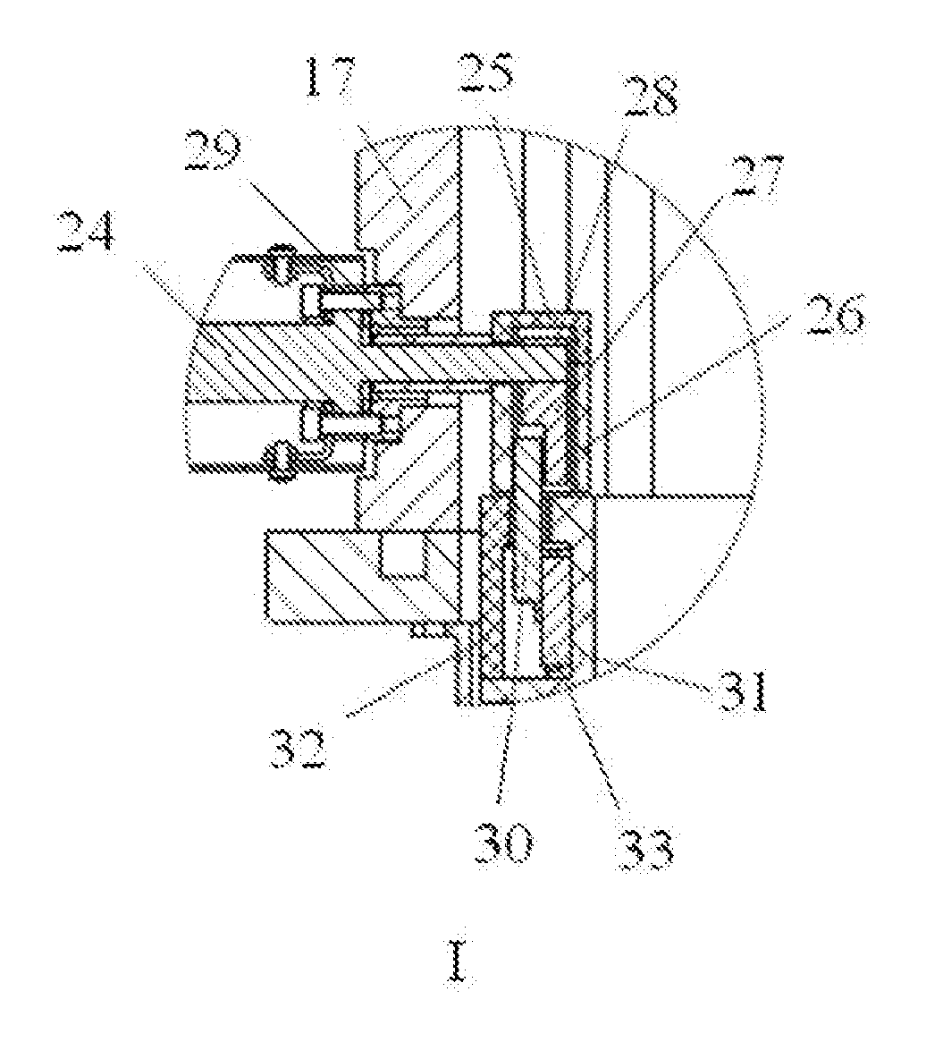
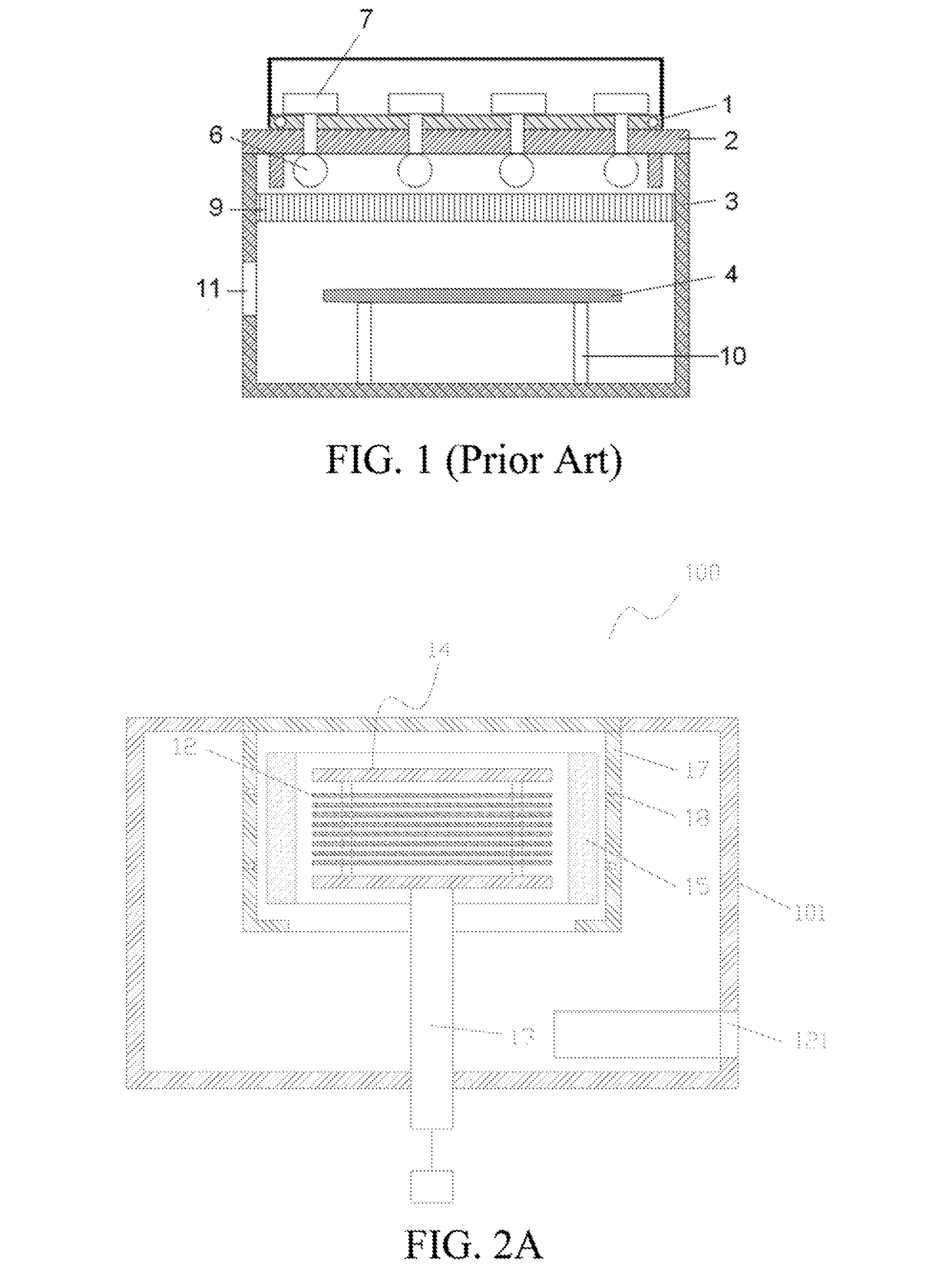
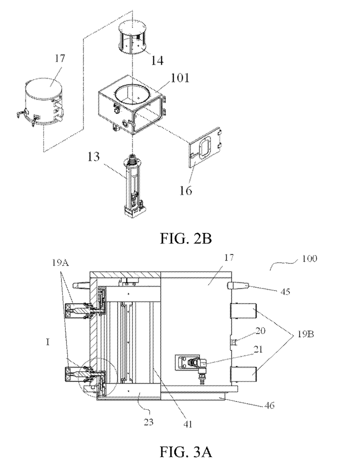
[0039]FIG. 2A is a cross-sectional view of a heating chamber provided by embodiments of the present disclosure. FIG. 2B is a schematic exploded diagram of a heating chamber provided by embodiments of the present disclosure. Referring to FIGS. 2A and 2B, the heating chamber 100 is defined by a chamber assembly 101, and has a vacuum environment aside. Further, the heating chamber 100 includes a heating barrel 17, an annular heating device 15, a substrate cassette 14 and a substrate cassette lifting device 13. Further, a substrate transferring window 121 allowing a substrate 12 to pass through is disposed in the chamber assembly 101 and below the heating barrel 17. The heating barrel 17 is disposed i...


PUM

PropertyMeasurementUnit
temperatureaaaaaaaaaa
electric currentaaaaaaaaaa
conductiveaaaaaaaaaa

Abstract

A heating chamber and a semiconductor processing apparatus are provided. The heating chamber includes: a heating barrel (17) disposed in the heating chamber and located above a substrate transferring window; an annular heating device (15) disposed around an inner side of the heating barrel and configured to radiate heat from a periphery to an interior of the heating barrel; a substrate cassette (14) configured to bear multiple layers of substrates and allow the multiple, layers of substrates to be arranged at intervals in an axial direction of the heating barrel; and a substrate cassette lifting device (13) configured to drive the substrate cassette to move up into an internal spare defined by the annular heating device, or move down to a position corresponding to the substrate transferring window.

Description

FIELD OF THE DISCLOSURE[0001]The present disclosure relates to the field of semiconductor apparatus manufacturing, and more particularly, relates to a heating chamber and a semiconductor processing apparatus.BACKGROUND[0002]The Physical Vapor Deposition (hereinafter referred to as PVD) technique is a processing technique commonly used in the field of microelectronics, and for example, PVD may be used to process a copper interconnection layer in an integrated circuit. Fabrication of a copper interconnection layer mainly includes steps such as degassing, pre-cleaning, deposition of Ta(N), and deposition of Cu, where the step of degassing is for removing water vapor and other volatile impurities on a to-be-processed workpiece such as a substrate. When the step of degassing is implemented, a heating chamber needs to be utilized to heat the to-be-processed workpiece such as a substrate to a temperature above 300° C.[0003]FIG. 1 is a structural schematic diagram of an existing beating cha...

Claims


Application Information

Patent Timeline
Patent Type & Authority Applications(United States)
IPC IPC(8): C23C14/54H01L21/67C23C14/50H05B3/00H01L21/677
CPCC23C14/541C23C14/50H05B3/0047H01L21/67757H01L21/67248H01L21/67109C23C14/02F27B17/0025H01L21/67115H01L21/6719
Inventor JIA, QIANGZHAO, MENGXIN
Owner BEIJING NAURA MICROELECTRONICS EQUIP CO LTD
Why Eureka
Try Eureka