High-power semiconductor laser based on vcsel and optical convergence method therefor

a semiconductor laser and optical convergence technology, applied in the direction of lasers, semiconductor laser arrangements, semiconductor lasers, etc., can solve the problems of fatal defects serious affecting the life of service, and the actual life of service of edge-emitting semiconductor lasers is far from the ideal expected life of service, etc., to achieve high reflectivity, high efficiency of secondary utilization, and effective transmission

a semiconductor laser and optical convergence technology, applied in the direction of lasers, semiconductor laser arrangements, semiconductor lasers, etc., can solve the problems of fatal defects serious affecting the life of service, and the actual life of service of edge-emitting semiconductor lasers is far from the ideal expected life of service, etc., to achieve high reflectivity, high efficiency of secondary utilization, and effective transmission

US20170331254A1Active Publication Date: 2017-11-16SANHE LASERCONN TECH CO LTD

Image

  • High-power semiconductor laser based on vcsel and optical convergence method therefor
  • High-power semiconductor laser based on vcsel and optical convergence method therefor
  • High-power semiconductor laser based on vcsel and optical convergence method therefor

Examples


Embodiment Construction

[0032]The technical content of the present invention is described in detail below with reference to the accompanying drawings and specific embodiments.

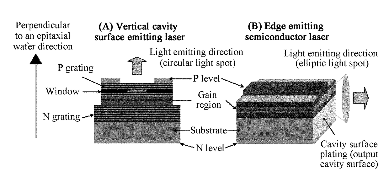
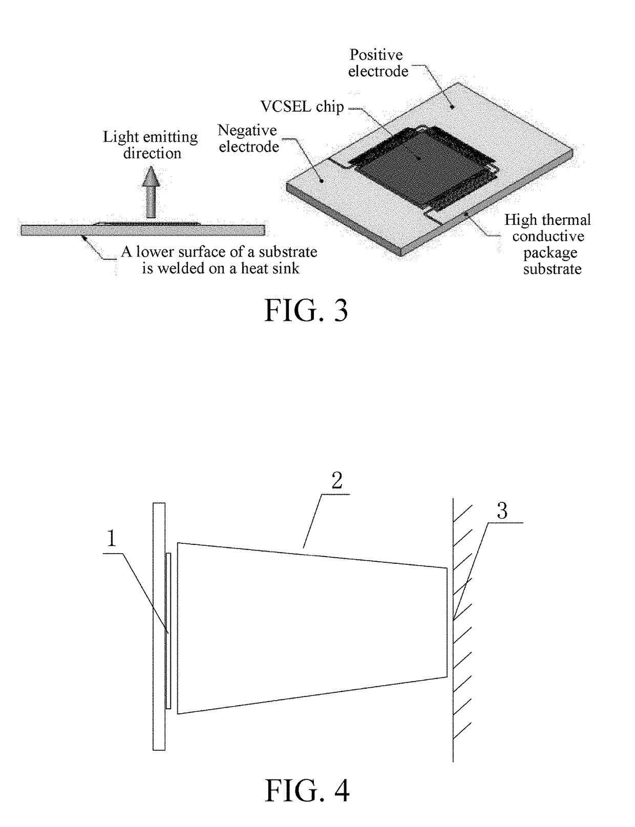
[0033]A high-power semiconductor laser provided in the present invention includes a VCSEL module according to either FIG. 4 or FIG. 7. The VCSEL module includes a VCSEL chip array 1 formed by multiple VCSEL chips and an inner wall reflective optical transmission device 2 disposed in front of a light emitting surface of the VCSEL chip array 1. The VCSEL chip array 1 and the inner wall reflective optical transmission device 2 are placed in front of a target object 3, and then a VCSEL is started, so as to implement a laser ablation function on the target object 3 by the VCSEL module. The inner wall reflective optical transmission device 2 may effectively transmit light rays emitted by the VCSEL chip array 1, to enable the light rays emitted by the VCSEL chip array 1 to focus on the target object 3. In addition, the inner wall reflective ...


PUM


Abstract

Provided is a high-power semiconductor laser based on VCSEL, comprising a VCSEL laser module. The VCSEL laser module includes a VCSEL chip array (1) consisting of a plurality of VCSEL chips (10) and an inner wall reflection optical transmission device (2) which is arranged in front of a light emergent face of the VCSEL chip array (1); and the light emergent face of the VCSEL chip array (1) is used for secondarily reflecting the reflected light reflected by a target object (3) and the inner wall reflection optical transmission device (2). Also provided is a packaging structure for the high-power semiconductor laser. The VCSEL chip array (1) is packaged by an inwardly concave arc-shaped heat sink (4), so that the purpose of converging the laser light beam near a centre position can be achieved.

Description

BACKGROUNDTechnical Field[0001]The present invention relates to a high-power semiconductor laser that uses a vertical cavity surface emitting laser (VCSEL) as a light source, and also to an optical convergence method for the high-power semiconductor laser, and belongs to the field of semiconductor laser technologies.Related Art[0002]Over the past twenty years, in the field of high-power semiconductor lasers, GaAs material-based edge-emitting semiconductor lasers have always been dominant, and have been widely applied to fields such as industry, medical treatment, and scientific research. However, the edge-emitting semiconductor lasers have fatal defects. Although an expected life of service of an edge-emitting semiconductor laser is up to tens of thousands of hours, the catastrophic optical damage probability of the edge-emitting semiconductor laser in a pulse status is extremely great, which seriously affects the life of service. Therefore, an actual life of service of the edge-emi...

Claims


Application Information

Patent Timeline
16 Nov 2017
Publication
US20170331254A1
IPC
H01S5/183; H01S5/42; H01S5/40
CPC
H01S5/18361; H01S5/4043; H01S5/426; H01S5/005; H01S5/02469; H01S5/4012; H01S5/423; H01S5/0225
Inventors
LI, YANG; LI, DELONG