

Ceramic capacitor
a ceramic capacitor and capacitor technology, applied in the field of ceramic capacitors, can solve the problems of multi-terminal capacitors, difficult to suitably embed multi-terminal capacitors, and inability to be embedded in substrates, and achieve the effect of reducing the path length of current flow and avoiding deformation
- Summary
- Abstract
- Description
- Claims
- Application Information
AI Technical Summary
Benefits of technology
Problems solved by technology
Method used
Image

Examples
second preferred embodiment
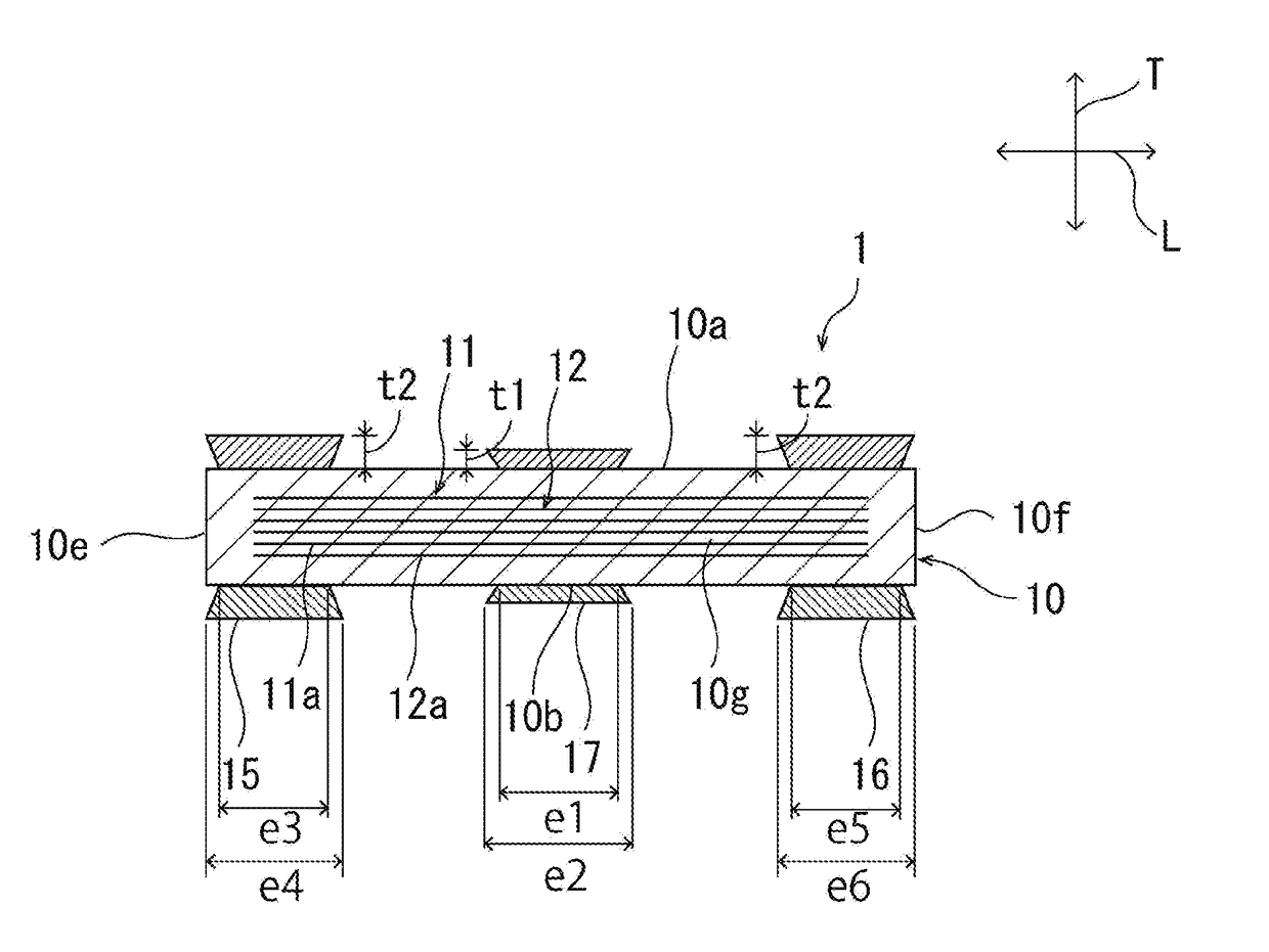
[0113]FIG. 10 is a schematic cross-sectional view of a capacitor of a second preferred embodiment of the present invention. FIG. 11 is a schematic cross-sectional view of a capacitor of the second preferred embodiment.
[0114]In the first preferred embodiment, an example in which the first and second external electrodes 15, 16 are not provided on the first and second end surfaces 10e, 10f, respectively, has been described. However, the present invention is not limited to this configuration.
[0115]For example, as shown in FIGS. 10 and 11, in a ceramic capacitor 1a, a first external electrode 15 extends over the first and second principal surfaces 10a, 10b / the first and second side surfaces 10c, 10d and portion of the first end surfaces 10e. The first external electrode 15 includes a first portion 15a, a second portion 15b, a third portion 15c, and a fourth portion 15d.
[0116]The first portion 15a extends from a portion located on the first principal surface 10a to a portion of the first...
example 1
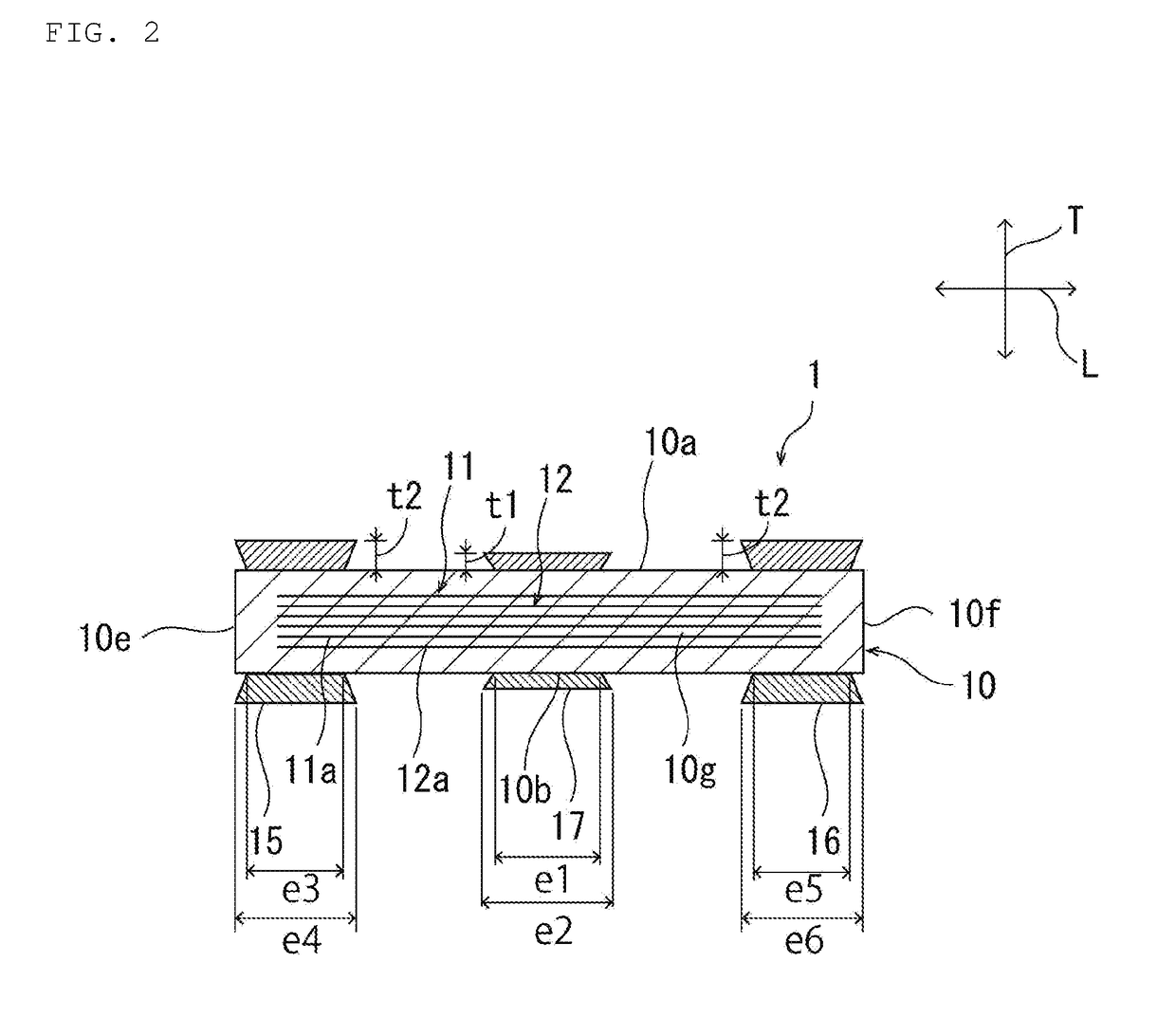
[0131]A plurality of capacitors having the substantially same constitution as in the ceramic capacitor 1 of the first preferred embodiment were prepared as samples of a ceramic capacitor under the following conditions using the production method described in the first preferred embodiment.[0132]Conditions:
[0133]Dimension of a ceramic capacitor (standard dimension):L×W×T=1.000 mm×0.600 mm×0.220 mm
[0134]Ceramic material: BaTi2O3
[0135]Capacitance: 1 μF
[0136]Rated voltage: 6.3 V
[0137]Structure of an external electrode: Base electrode layer / thin film electrode layer / plated layer
[0138]Base electrode layer: Ni fired electrode layer
[0139]Thin film electrode layer: NiCr sputtering film / NiCu sputtering film
[0140]Plated layer: one Cu plated layer
[0141]Thickness of Base electrode layer (central portion): 6 μm
[0142]Thickness of a thin film electrode layer (central portion): total 0.3 μm (each layer 0.15 μm)
[0143]Thickness of a plated layer (central portion): 10 μm
[0144]e1: 230 μm
[0145]e2: 250 μ...
examples 2 to 8
[0157]A plurality of capacitors having the substantially same constitution as in the ceramic capacitor 1 of the first preferred embodiment were prepared as samples of a ceramic capacitor under the following conditions using the production method described in the first preferred embodiment.
Conditions:
[0158]Dimension of a ceramic capacitor (standard dimension):L×W×T=1.000 mm×0.600 mm×0.220 mm
[0159]Ceramic material: BaTi2O3
[0160]Capacitance: 1 μF
[0161]Rated voltage: 6.3 V
[0162]Structure of an external electrode: Base electrode layer / thin film electrode layer / plated layer
[0163]Base electrode layer: Ni fired electrode layer
[0164]Thin film electrode layer: NiCr sputtering film / NiCu sputtering film
[0165]Plated layer: one Cu plated layer
[0166]Thickness of Base electrode layer (central portion): 6 μm
[0167]Thickness of a thin film electrode layer (central portion): total 0.3 μm (each layer 0.15 μm)
[0168]Thickness of a plated layer (central portion): 10 μm
[0169]e2: 250 μm
[0170]e4: 250 μm
[0171...
PUM
| Property | Measurement | Unit |
|---|---|---|
| thickness | aaaaa | aaaaa |
| thickness | aaaaa | aaaaa |
| thickness | aaaaa | aaaaa |
Abstract
Description
Claims
Application Information