Method for producing patterns

a pattern and pattern technology, applied in the field of structures, can solve the problems of reducing the dimensions of patterns, limiting the choice of surface profiles that can be obtained, and reducing the accuracy of techniques, etc., to achieve the effect of not consuming the thickness of the masking layer, simple and reliable solution, and great precision

Active Publication Date: 2017-11-30
COMMISSARIAT A LENERGIE ATOMIQUE ET AUX ENERGIES ALTERNATIVES
View PDF5 Cites 7 Cited by
  • Summary
  • Abstract
  • Description
  • Claims
  • Application Information

AI Technical Summary

Benefits of technology

[0034]The invention as such makes it possible to obtain a structure of which the profile is free of the aligning defects that are usually encountered with the known methods that require successive operations of lithography.
[0035]Moreover, with respect to a solution wherein the layer to be etched would be implanted in line with a hollow pattern made in the masking layer, then wherein the patterns would be enlarged via trimming before the new implantation over a lower depth, the invention has for advantage to not consume a thickness of the masking layer between two implantations. Consequently, the depth of the implantations is controlled with great precision.
[0036]The invention as such offers a simple and reliable solution for obtaining a profile that is possibly complex and which has an improved definition, optionally by repeating several times said sequence of steps b1) and b2) before the steps d) and e) of removing the masking layer and of removing the modified areas.

Problems solved by technology

The constant reduction on the dimensions of patterns then poses the difficulty of managing to effectively align the patterns with enough precision during successive operations of photolithography.
This problem is particularly important for the production of microlens arrays used in many optoelectronic devices.
However, these techniques are more qualitative than quantitative when it entails reaching a predetermined surface profile intended to provide the lenses with the expected optical properties.
For example, thermal reflow of photo-resin and microjet printing are based on the surface tensions which substantially limit the choice of the surface profiles that can be obtained in practice with these techniques.
This results in that these techniques are not applicable in terms of costs and output at an industrial scale.
Although the methods of manufacturing the mold briefly described hereinabove are suitable for the obtaining, as represented by spherical or hemispherical patterns, it is however difficult to obtain so-called aspherical lenses of a desired shape with these methods.
In particular, spherical lenses, contrary to aspherical lenses, induce optical aberrations, with the rays passing through the center of the lens not converging exactly at the same point as those passing through the edges.
This causes a blur with large openings and an enlargement of the focusing spot that is not possible to ignore in most applications.
Recourse must then be had to the use of lasers and so-called “laser machining” or laser ablation techniques, already mentioned hereinabove, which alone are able to create the complex profiles required with however the major disadvantage that each microlens then has to be shaped individually.
Generally, there is no simple and fast method, i.e. which can work in a single series of steps on the scale of a wafer, also compatible with the standard techniques of microelectronics and which makes it possible to simply control the surface profile with the purpose of producing in particular aspherical lens arrays.
The standard method that makes it possible to produce these 3D structures exhibiting steps is complicated and requires a substantial number of steps as is shown in FIGS. 3a to 3f.
A particular difficulty consists in being able to precisely align successive steps of structuring in relation to one another.
The presence of such defects is obviously very detrimental and no longer makes it possible to obtain the final profile sought.

Method used


Image

  • Method for producing patterns
  • Method for producing patterns
  • Method for producing patterns

Examples


Embodiment Construction

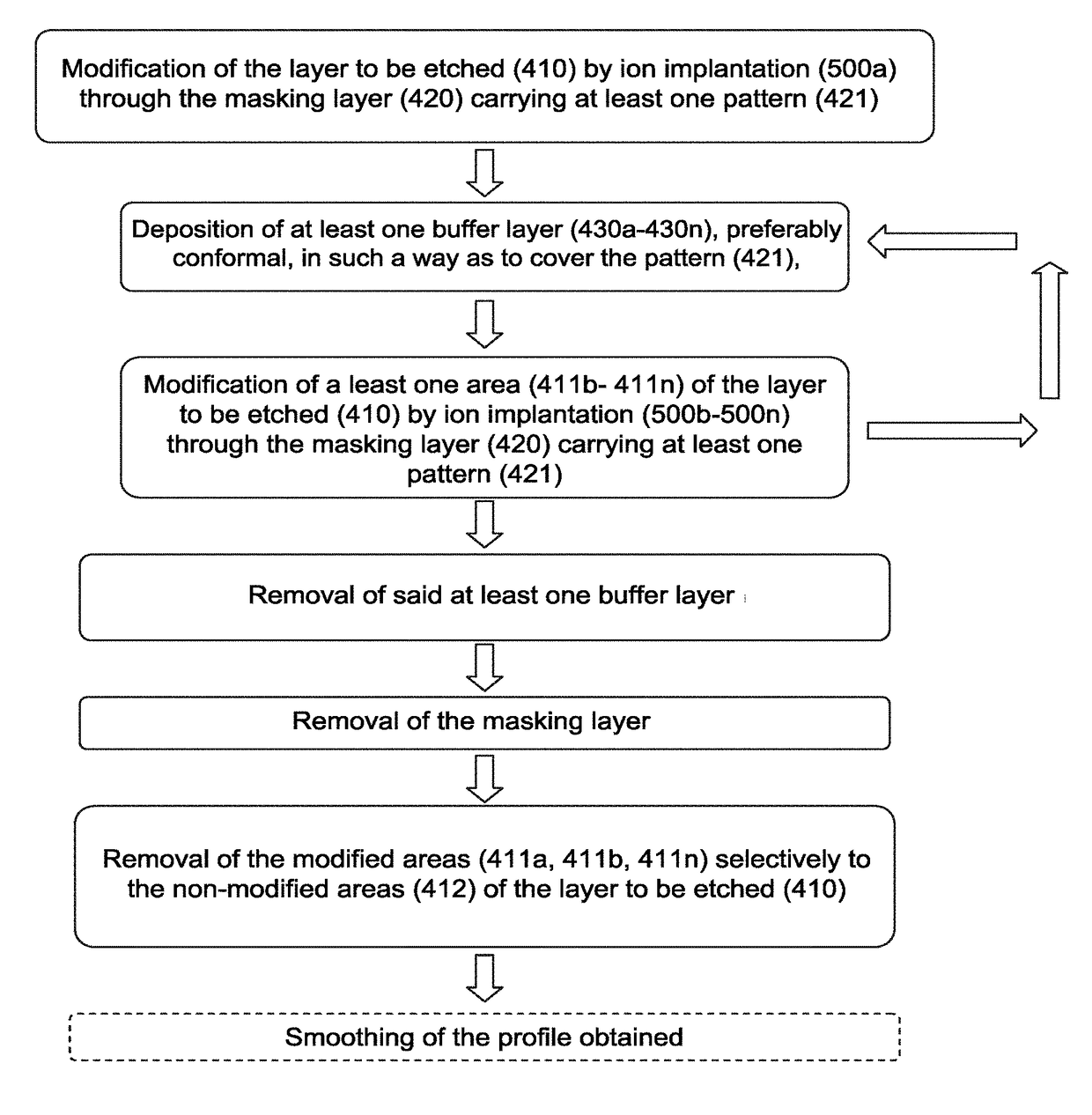
[0048]Before beginning a detailed review of embodiments of the invention, hereinafter are mentioned optional characteristics that can possibly be used in association or alternatively.

[0049]According to an embodiment, before the step c) of removing said at least one buffer layer, several times, more preferably at least two times and more preferably at least three times, a sequence of steps is carried out, with each sequence comprising the steps b1) and b2), with a buffer layer deposited during a given sequence being stacked as such on a buffer layer deposited during a sequence preceding the given sequence.

[0050]As such the buffer layers deposited are stacked on one another as the sequences unfold.

[0051]According to an embodiment a buffer layer deposited during a given sequence has a thickness that is identical to the thickness of a buffer layer deposited during a sequence preceding the given sequence. This avoids having to adjust the thickness to be deposited for each buffer layer, w...


PUM


Abstract

A method for producing patterns in a layer to be etched, from a stack including at least the layer to be etched and a masking layer overlying the layer to be etched, with the masking layer having at least one pattern. The method includes modifying a first area of the layer to be etched by ion implantation through the masking layer; depositing a buffer layer to cover the pattern of the masking layer; modifying another area of the layer to be etched, different from the first area, by ion implantation through the buffer layer, to a depth of the layer to be etched greater than the implantation depth of the preceding step of modifying; removing the buffer layer; removing the masking layer; removing the modified areas by etching them selectively to the non-modified areas of the layer to be etched.

Description

TECHNICAL FIELD OF THE INVENTION[0001]The invention in general relates to the production of structures in the field of methods used by the microelectronics industry for the manufacture of all sorts of systems, of micrometric and nanometric size, possibly combining electronic, optical and mechanical components.[0002]More precisely, it relates to methods in which it is necessary to align patterns with respect to other patterns produced beforehand.[0003]The invention has for particularly advantageous application the production of aspherical microlenses intended for light collecting applications, imaging and guiding light. It also has as an advantageous application the production of structures referred to as “dual damascene” for the vertical interconnection of metal lines in particular made of copper.PRIOR ART[0004]For many applications, it is necessary to produce patterns aligned on other patterns defined beforehand during preceding operations of photolithography and etching.[0005]The ...

Claims


Application Information

Patent Timeline
Patent Type & Authority Applications(United States)
IPC IPC(8): H01L21/02H01L21/033H01L21/3213
CPCH01L21/02694H01L21/02304H01L21/033H01L21/3213G02B3/0012G03F7/0005H01L21/30608H01L21/3083
Inventor POSSEME, NICOLASLANDIS, STEFANNOURI, LAMIA
Owner COMMISSARIAT A LENERGIE ATOMIQUE ET AUX ENERGIES ALTERNATIVES
Why Eureka
Try Eureka