Organic Light Emitting Diode Comprising an Organic Semiconductor Layer

a light-emitting diode and organic technology, applied in the direction of organic semiconductor devices, solid-state devices, semiconductor devices, etc., can solve the problems of poor performance and carrier balance may not be maintained, and achieve the effect of improving working device yield, reducing the number of layers and compounds in the device, and improving the operating voltag

Active Publication Date: 2017-11-30
NOVALED GMBH
View PDF1 Cites 8 Cited by
  • Summary
  • Abstract
  • Description
  • Claims
  • Application Information

AI Technical Summary

Benefits of technology

[0006]Therefore, it is the object of the present invention to provide OLEDs with transparent cathodes overcoming drawbacks of the prior art, in particular having improved operating voltage, improved yield of working devices and / or a reduced number of layers and compounds in the device.

Problems solved by technology

However, there is the problem of such organic light-emitting diodes that the same suffer from poor performance which may be deduced to the damage caused to underlying layers through sputtering processes, in particular if the underlying layers comprise a metal dopant.
As a result, a carrier balance may not be maintained, so as to reduce the lifetime of the OLED.

Method used


Image

  • Organic Light Emitting Diode Comprising an Organic Semiconductor Layer
  • Organic Light Emitting Diode Comprising an Organic Semiconductor Layer
  • Organic Light Emitting Diode Comprising an Organic Semiconductor Layer

Examples


examples

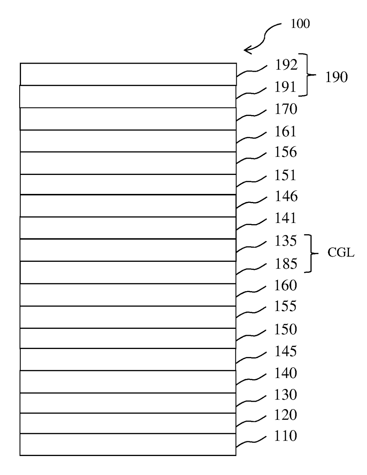
[0249]First matrix compounds comprising at least two phenanthrolinyl groups can be synthesized as described in JP2002352961.

Top Emission Devices

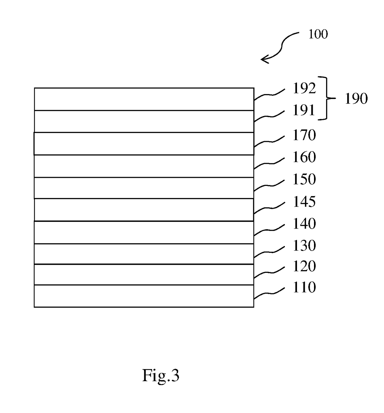
[0250]For top emission devices—Examples 1 to 3 and comparative examples 1 to 7, a glass substrate was cut to a size of 50 mm×50 mm×0.7 mm, ultrasonically cleaned with isopropyl alcohol for 5 minutes and then with pure water for 5 minutes, and cleaned again with UV ozone for 30 minutes. Then, 100 nm Ag was deposited on the glass substrate to form the first anode electrode.

[0251]Then, 92 wt.-% of Biphenyl-4-yl(9,9-diphenyl-9H-fluoren-2-yl)-[4-(9-phenyl-9H-carbazol-3-yl)phenyl]-amine (CAS 1242056-42-3) and 8 wt.-% of 2,2′,2″-(cyclopropane-1,2,3-triylidene)tris(2-(p-cyanotetrafluorophenyl)acetonitrile) was vacuum deposited on the anode electrode, to form a HIL having a thickness of 10 nm. Then Biphenyl-4-yl(9,9-diphenyl-9H-fluoren-2-yl)-[4-(9-phenyl-9H-carbazol-3-yl)phenyl]-amine was vacuum deposited on the HIL, to form a HTL having a thickness ...


PUM


Abstract

The present invention relates to organic light-emitting diodes that include an anode electrode, a transparent cathode electrode, at least one emission layer and at least one organic semiconductor layer, wherein the at least one emission layer and the at least one organic semiconductor layer is arranged between the anode electrode and the transparent cathode electrode and the organic semiconductor layer includes a first zero-valent metal dopant and a first matrix compound wherein the first matrix comprising at least two phenanthrolinyl groups as well as to a method for manufacturing the same.

Description

[0001]The present invention relates to an organic light emitting diode (OLED) comprising a transparent cathode electrode and an organic semiconductor layer, a compound of formula 1 comprised therein and a method of manufacturing the organic light emitting diode (OLED) comprising the organic semiconductor layer.DESCRIPTION OF THE RELATED ART[0002]Organic light emitting diodes (OLEDs), which are self-emitting devices, have a wide viewing angle, excellent contrast, quick response, high brightness, excellent driving voltage characteristics, and color reproduction. A typical OLED includes an anode electrode, a hole injection layer (HIL), a hole transport layer (HTL), an emission layer (EML), an electron transport layer (ETL), and a cathode electrode, which are sequentially stacked on a substrate. In this regard, the HIL, the HTL, the EML, and the ETL are thin films formed from organic compounds.[0003]When a voltage is applied to the anode electrode and the cathode electrode, holes inject...

Claims


Application Information

Patent Timeline
Patent Type & Authority Applications(United States)
IPC IPC(8): H01L51/00H01L51/52H01L51/50H01L51/56
CPCH01L51/0072H01L51/5234H01L51/504H01L51/0021H01L51/56H01L51/006H01L51/0052H01L51/0058H01L51/0071H01L2251/558H01L51/5012H01L51/5076H01L51/0002H01L51/0061H10K85/6572H10K50/828H10K71/00H10K71/611H10K71/30H10K85/351H10K50/12H10K50/157H10K71/60H10K85/654H10K85/657H10K50/11H10K50/13H10K85/626H10K85/633H10K85/636H10K50/165H10K71/10H10K85/615H10K2102/351
Inventor JANKUS, VYGINTASROTHE, CARSTEN
Owner NOVALED GMBH
Why Eureka
Try Eureka