Optical semiconductor device

Active Publication Date: 2017-11-30
SONY CORP
View PDF2 Cites 6 Cited by
  • Summary
  • Abstract
  • Description
  • Claims
  • Application Information

AI Technical Summary

Benefits of technology

[0012]In the optical semiconductor device according to the first to third aspects of the present disclosure, as tunnel barrier layers are provided, electrons are distributed unevenly such that many electrons are present at the side of the p-type compound semiconductor layer. As a result, the emission peak wavelength or the optical gain peak wavelength of a well layer adjacent to the p-type compound semiconductor layer differs from that of another well layer. Specifically, these wavelengths of the well layer adjacent to the p-type compound semiconductor layer are shortened. The compositional variation of a well layer adjacent to the p-type compound semiconductor layer is greater than the compositional variation of another well layer in the optical semiconductor device according to the first aspect of the present disclosure, the band gap energy of a well layer

Problems solved by technology

However, in a nitride compound semiconductor light emitting device which emits blue or green light, the amount of current injected increases as the emission wavelength increases, which causes problems such as a reduction in the emission efficiency and an increase in the threshold current.
One cause of these problems is non-uniformity of carriers in an active layer (i.e., a light emitting layer).
In addition, when an active layer is formed on a c-surface of a GaN substrate, piezoelectric field effects occur in well or barrier layers such that it is difficult for carriers (electrons or holes) to exit a well layer once they have entered the well layer, thus causing non-uniform

Method used


Image

  • Optical semiconductor device
  • Optical semiconductor device
  • Optical semiconductor device

Examples


Example

Embodiment 1

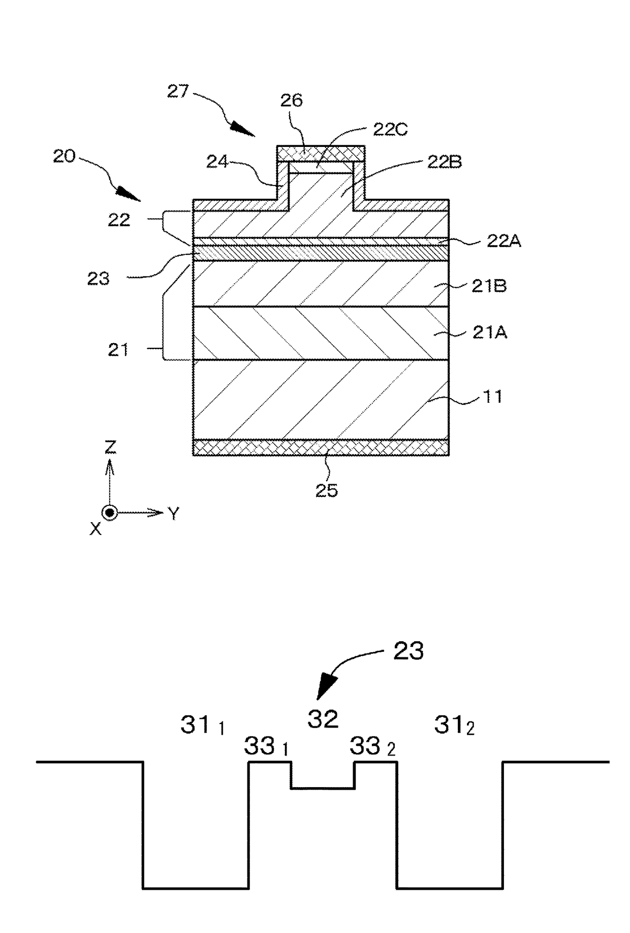
[0058]Embodiment 1 relates to an optical semiconductor device, specifically to a semiconductor laser device (LD), according to the first aspect of the present disclosure. FIG. 1A is a schematic partial sectional view of an optical semiconductor device of embodiment 1, specifically a schematic partial sectional view of an optical semiconductor device taken along a virtual plane (YZ plane) perpendicular to the extending direction of a resonator and FIG. 1B is a schematic structural view of a multiquantum well structure in an active layer. FIG. 1B shows a band structure without considering the influence of piezoelectric fields for the sake of convenience.

[0059]The semiconductor optical device of embodiment 1 or embodiments 1 to 10 described later has a laminate structural body 20 in which an n-type compound semiconductor layer 21, an active layer 23, and a p-type compound semiconductor layer 22 are laminated in this order. The active layer 23 includes a multiquantum well st...

Example

Embodiment 2

[0069]Embodiment 2 relates to an optical semiconductor device, specifically to a semiconductor laser device (LD), according to the second aspect of the present disclosure. In the optical semiconductor device of embodiment 2, the band gap energy of a well layer (the second well layer 312) adjacent to the p-type compound semiconductor layer is smaller than the band gap energy of another well layer (specifically, the first well layer 311) (see Table 4). Here, it is assumed that the configuration of an active layer 23 in the optical semiconductor device of embodiment 2 is as in Table 3. The emission wavelength of the semiconductor laser device of embodiment 2 is equal to or greater than 440 nm and is specifically 460 nm. Specifically, the band gap energy of the well layer (the second well layer 312) adjacent to the p-type compound semiconductor layer can be made smaller than the band gap energy of another well layer (specifically, the first well layer 310 by allowing the amo...

Example

Embodiment 3

[0071]Embodiment 3 relates to an optical semiconductor device, specifically to a semiconductor laser device (LD), according to the third aspect of the present disclosure. In the optical semiconductor device of embodiment 3, the thickness of a well layer (the second well layer 312) adjacent to the p-type compound semiconductor layer is greater than the thickness of another well layer (specifically, the first well layer 311). Here, it is assumed that the configuration of an active layer 23 in the optical semiconductor device of embodiment 3 is as in Table 5. The emission wavelength of the semiconductor laser device of embodiment 3 is equal to or greater than 440 nm and is specifically 460 nm. Specifically, the thickness of the well layer (the second well layer 312) adjacent to the p-type compound semiconductor layer can be made greater than the thickness of another well layer (specifically, the first well layer 311) by allowing the deposition time of the second well layer ...


PUM


Abstract

Provided is an optical semiconductor device including a laminate structural body 20 in which an n-type compound semiconductor layer 21, an active layer 23, and a p-type compound semiconductor layer 22 are laminated in this order. The active layer 23 includes a multiquantum well structure including a tunnel barrier layer 33, and a compositional variation of a well layer 312 adjacent to the p-type compound semiconductor layer 22 is greater than a compositional variation of another well layer 311. Band gap energy of the well layer 312 adjacent to the p-type compound semiconductor layer 22 is smaller than band gap energy of the other well layer 311. A thickness of the well layer 312 adjacent to the p-type compound semiconductor layer 22 is greater than a thickness of the other well layer 311.

Description

TECHNICAL FIELD[0001]The present disclosure relates to an optical semiconductor device.BACKGROUND ART[0002]Increase of the emission efficiency and reduction of the threshold current in various light emitting diodes or semiconductor laser devices are essential for high output and improvement of power consumption or the like and are currently being intensively investigated. However, in a nitride compound semiconductor light emitting device which emits blue or green light, the amount of current injected increases as the emission wavelength increases, which causes problems such as a reduction in the emission efficiency and an increase in the threshold current. One cause of these problems is non-uniformity of carriers in an active layer (i.e., a light emitting layer). That is, the energy gap difference between barrier and well layers which constitute a multiquantum well structure increases as the emission wavelength increases. In addition, when an active layer is formed on a c-surface of...

Claims


Application Information

Patent Timeline
IPC IPC(8): H01S5/343H01S5/183H01S5/22H01L33/06H01L33/32H01S5/042
CPCH01S5/34333H01S5/183H01S5/22H01S5/0425H01L33/32H01S2304/04H01L33/06H01L21/02389H01L21/02433H01L21/0254H01L21/02576H01L21/02579H01L21/0262H01S5/0287H01S5/04252H01S5/04254H01S5/305H01S5/3063H01S5/3407H01S5/3416H01S2301/176H01S5/343
Inventor KURAMOTO, MASARUFUTAGAWA, NORIYUKIHAMAGUCHI, TATSUSHIIZUMI, SHOICHIRO
Owner SONY CORP
Why Eureka
Try Eureka