Complementary metal oxide semiconductor (CMOS) devices employing plasma-doped source/drain structures and related methods

a metal oxide semiconductor and source/drain technology, applied in the direction of semiconductor devices, electrical apparatus, transistors, etc., can solve the problems of increasing current leakage, degrading performance, and complex functionality of electronic devices, so as to reduce the width of the channel structure, shorten the adjacent channel structure, and reduce the contact resistance of the channel

Inactive Publication Date: 2017-12-07
QUALCOMM INC
View PDF3 Cites 13 Cited by
  • Summary
  • Abstract
  • Description
  • Claims
  • Application Information

AI Technical Summary

Benefits of technology

[0010]Aspects disclosed in the detailed description include complementary metal oxide semiconductor (CMOS) devices employing plasma-doped source / drain structures and related methods. In certain aspects, a source and a drain of a CMOS device are formed at end portions of a channel structure by plasma doping end portions of the channel structure. In particular, the end portions of the channel structure are plasma-doped above a solid state solubility of the channel structure and annealed for liquid phase epitaxy and activation (e.g., superactivation) to form the source and drain of the CMOS device. In this manner, the source and drain can be integrally formed in the end portions of the channel structure to provide coextensive surface area contact between the source and drain and the channel structure to provide lower channel contact resistance. This is opposed to, for example, a source and drain formed using epitaxial growth that provides an overgrowth beyond the end portions of a surface area of the channel structure to offset a scaled down layout design with a reduced channel structure width, and which may then risk shorting adjacent channels structures at a scaled down channel structure pitch. Further, by providing integrally formed source and drains in the end portions of the channel structure, a stressed contact fill metal may be more easily disposed on the source and drain adjacent to the channel structure to enhance channel strain on the channel structure to increase carrier mobility performance.

Problems solved by technology

As electronic devices become more complex in functionality, so does the need to include a greater number of transistors in such devices.
In particular, as channel length in planar transistors is reduced such that the channel length is of the same order of magnitude as depletion layer widths, short channel effects (SCEs) can occur that degrade performance.
More specifically, SCEs in planar transistors cause increased current leakage, reduced threshold voltage, and / or threshold voltage roll-off (i.e., reduced threshold voltage at shorter gate lengths), and therefore, reduced gate control.
Contact resistance is a limiting factor in fabrication of CMOS devices, with high contact resistance resulting in degradation of performance, errors in data, and increase heat and power loss, to name a few effects.
Further scaling down of CMOS devices, however, has reduced the effective epitaxial growth of source / drain regions.
This increases contact resistance, which may result in loss of performance, errors in data, and increased heat and power loss, to name a few effects.
However, reducing the fin width 126 also reduces the contact area between the source / drain region and a corresponding channel structure which, as noted earlier, increases contact resistance and may result in loss of performance, errors in data, and increased heat and power loss.
This, in turn, makes it difficult for the source / drain region to have the necessary mechanical support in the fin 104A, 104B to provide an adequate channel strain to the channel structure therein, resulting in a weaker channel strain, and thus reducing mobility and speed of the transistor.

Method used


Image

  • Complementary metal oxide semiconductor (CMOS) devices employing plasma-doped source/drain structures and related methods
  • Complementary metal oxide semiconductor (CMOS) devices employing plasma-doped source/drain structures and related methods
  • Complementary metal oxide semiconductor (CMOS) devices employing plasma-doped source/drain structures and related methods

Examples


Embodiment Construction

[0030]With reference now to the drawing figures, several exemplary aspects of the present disclosure are described. The word “exemplary” is used herein to mean “serving as an example, instance, or illustration.” Any aspect described herein as “exemplary” is not necessarily to be construed as preferred or advantageous over other aspects.

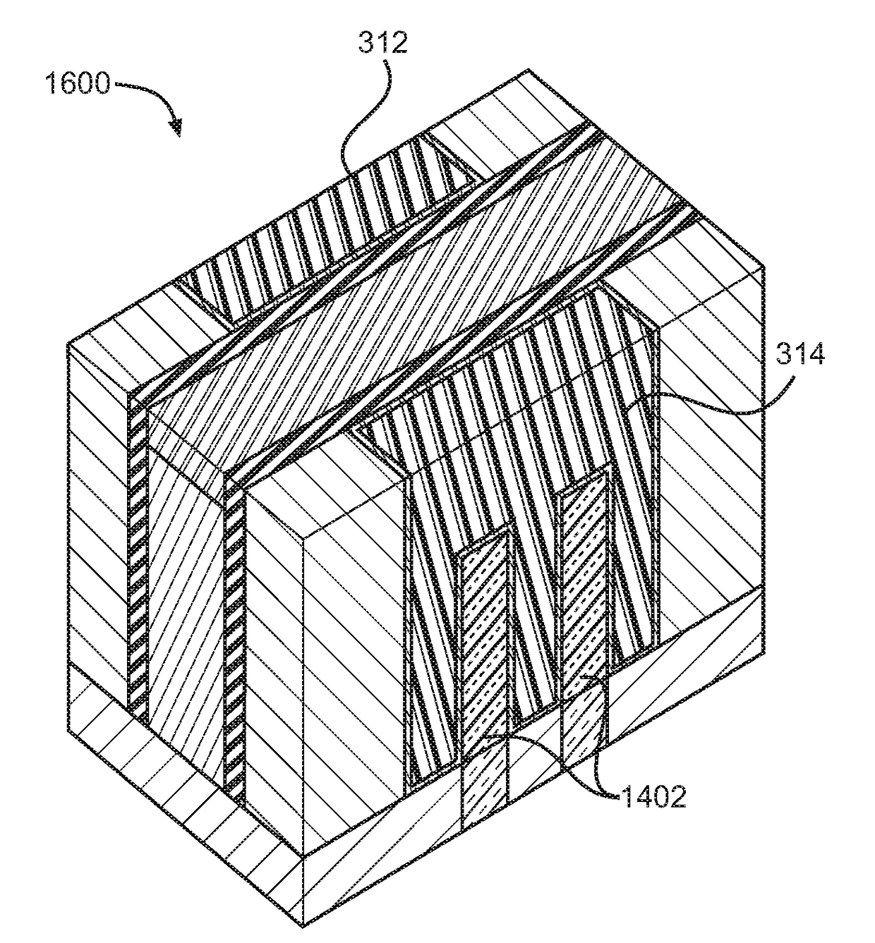
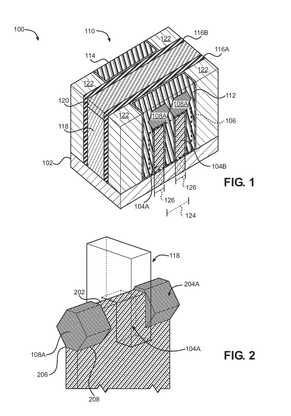
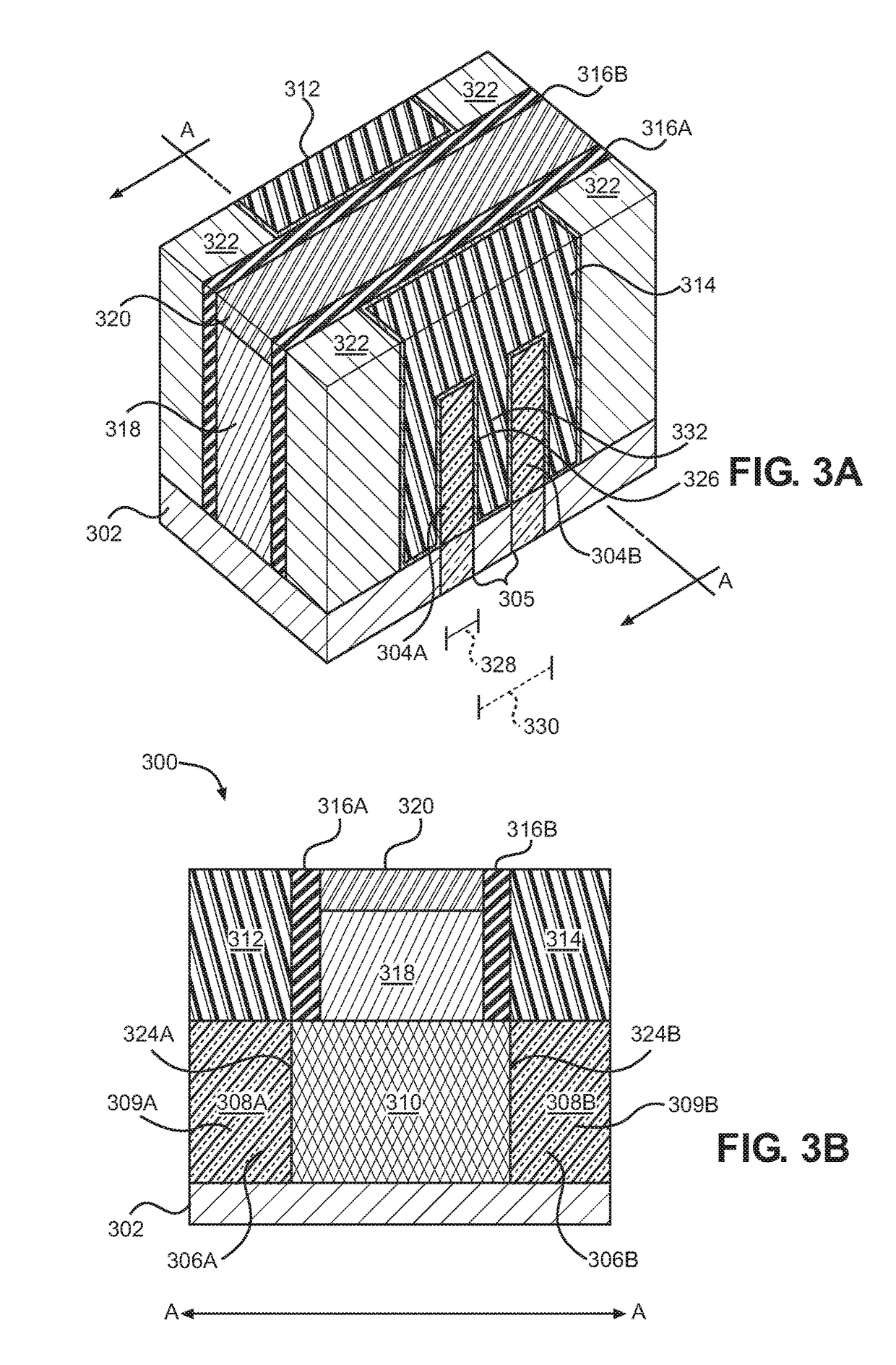
[0031]Aspects disclosed in the detailed description include complementary metal oxide semiconductor (CMOS) devices employing plasma-doped source / drain structures and related methods. In certain aspects, a source and a drain of a CMOS device are formed at end portions of a channel structure by plasma doping end portions of the channel structure. In particular, the end portions of the channel structure are plasma-doped above a solid state solubility of the channel structure and annealed for liquid phase epitaxy and activation (e.g., superactivation) to form the source and drain of the CMOS device. In this manner, the source and drain can be integrally f...


PUM


Abstract

Complementary metal oxide semiconductor (CMOS) devices employing plasma-doped source/drain structures and related methods are disclosed. In certain aspects, a source and drain of a CMOS device are formed at end portions of a channel structure by plasma doping end portions of the channel structure above solid state solubility of the channel structure, and annealing the end portions for liquid phase epitaxy and activation (e.g., superactivation). In this manner, the source and drain can be integrally formed in the end portions of the channel structure to provide coextensive surface area contact between the source and drain and the channel structure for lower channel contact resistance. This is opposed to forming the source/drain using epitaxial growth that provides an overgrowth beyond the end portion surface area of the channel structure to reduce channel contact resistance, which may short adjacent channels structures.

Description

PRIORITY CLAIM[0001]The present application claims priority under 35 U.S.C. §119(e) to U.S. Provisional Patent Application Ser. No. 62 / 345,335 filed on Jun. 3, 2016 and entitled “COMPLEMENTARY METAL OXIDE SEMICONDUCTOR (CMOS) DEVICES EMPLOYING PLASMA-DOPED SOURCE / DRAIN STRUCTURES,” the contents of which is incorporated herein by reference in its entirety.BACKGROUNDI. Field of the Disclosure[0002]The technology of the disclosure relates generally to fabrication of complementary metal oxide semiconductor (CMOS) devices, and more specifically, to forming source / drain structures in CMOS devices.II. Background[0003]Transistors are essential components in modern electronic devices, and large numbers of transistors are employed in integrated circuits (ICs) therein. For example, components such as central processing units (CPUs) and memory systems each employ a large quantity of transistors for logic circuits and memory devices.[0004]As electronic devices become more complex in functionalit...

Claims


Application Information

Patent Timeline
Patent Type & Authority Applications(United States)
IPC IPC(8): H01L27/092H01L21/8234H01L29/66H01L29/417H01L29/78
CPCH01L27/0924H01L29/41791H01L29/7851H01L21/823431H01L2029/7858H01L21/823437H01L21/823468H01L29/66545H01L21/823475H01L21/823807H01L21/823821H01L21/823871H01L29/0847H01L29/66803H01L29/7845
Inventor XU, JEFFREY JUNHAO
Owner QUALCOMM INC
Why Eureka
Try Eureka