Approach for an Area-Efficient and Scalable CMOS Performance Based on Advanced Silicon-On-Insulator (SOI), Silicon-On-Sapphire (SOS) and Silicon-On-Nothing (SON) Technologies

Active Publication Date: 2017-12-14
TARAKJI AHMAD HOUSSAM
View PDF0 Cites 4 Cited by
  • Summary
  • Abstract
  • Description
  • Claims
  • Application Information

AI Technical Summary

Benefits of technology

[0034]FIG. 12: Simulation of the Body potential in a fully optimized large-periphery 1-leg FD-SOI NMOS. It exhibited less than a 0.1V throughout its P_Body. The device was optimized in the back-accumulation mode (with an applied negative bias to its Back-Gate, in addition to the positive bias for inversion at the Front-Gate). These boosted further the conductance that the Impact-Ionizations current sees between the P_Body and the BTS. WB=0.5 μm.
[0035]FIG. 13: Measured and simulated Current-Voltage transfer curves of FD-SOI NMOS devices (WGeff=2 μm; LG=0.35 μm; VD=3.3V); Box=0.5 μm; CFox-10 nm;

Problems solved by technology

This consequently results in lowest possible voltage-drop

Method used


Image

  • Approach for an Area-Efficient and Scalable CMOS Performance Based on Advanced Silicon-On-Insulator (SOI), Silicon-On-Sapphire (SOS) and Silicon-On-Nothing (SON) Technologies
  • Approach for an Area-Efficient and Scalable CMOS Performance Based on Advanced Silicon-On-Insulator (SOI), Silicon-On-Sapphire (SOS) and Silicon-On-Nothing (SON) Technologies
  • Approach for an Area-Efficient and Scalable CMOS Performance Based on Advanced Silicon-On-Insulator (SOI), Silicon-On-Sapphire (SOS) and Silicon-On-Nothing (SON) Technologies

Examples


Embodiment Construction

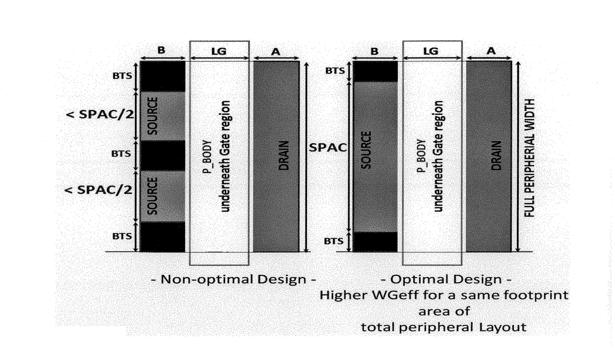
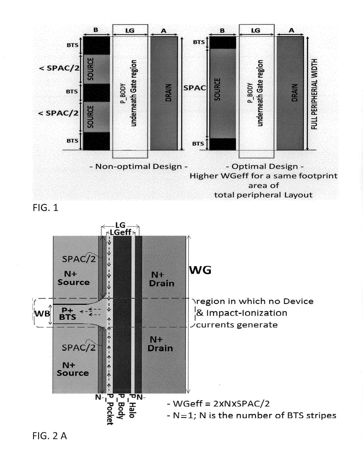
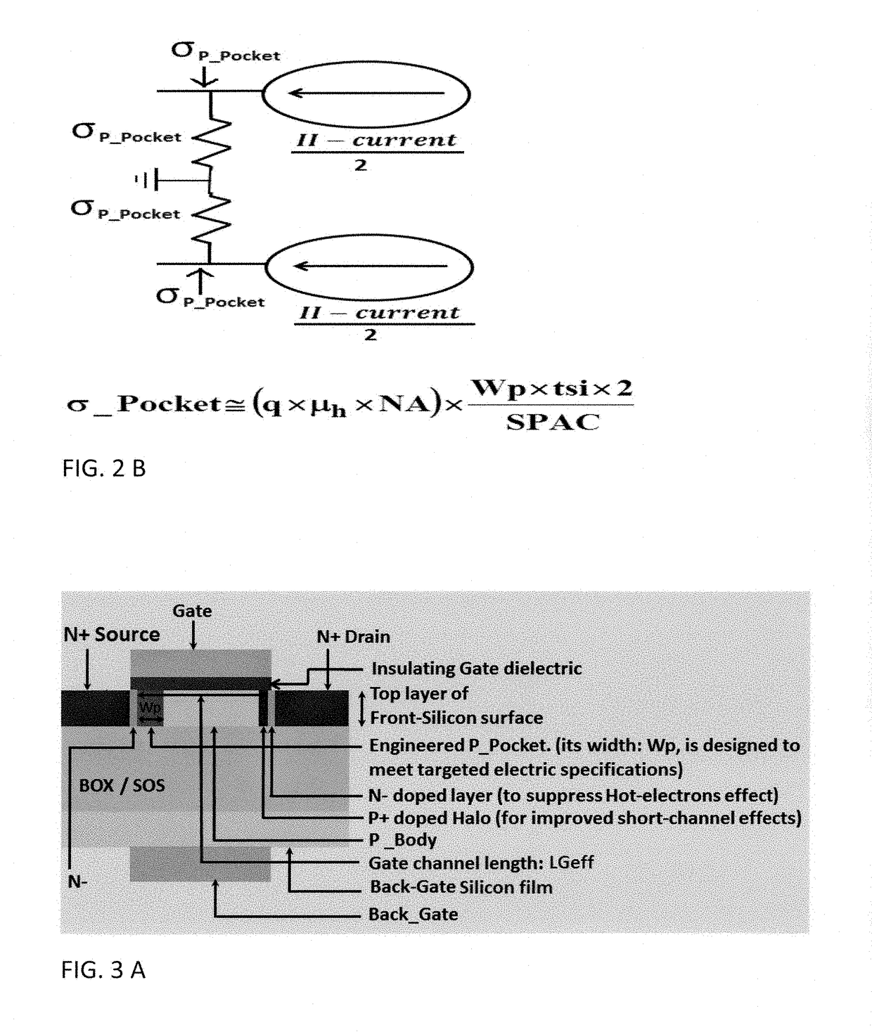
[0037]A top-view of such device layout is depicted in FIG. 2 A. Further schematics describing its structures are shown in FIG. 3 A, FIG. 3 B, and FIG. 3 C. The P_Pocket extends from the Source into the “effective” Gate-Length of the device (LGeff) a distance: Wp that is a relatively small fraction of LGeff so to ensure the P_Pocket is conductive enough and with no or little penalty on the device VT. A tighter or a more loose constraint on Wp may always be set for the specific application. As is shown with the dashed-arrows in FIG. 2 A, the device structure splits the II-current that generates around its Drain's edge into two equal magnitudes that converge through separate paths to the BTS while conducting in P_Pocket alongside the Gate-width of the structure. FIG. 2 B shows an equivalent circuit diagram depicting the flow of Impact-Ionizations current (II-current) to the BTS. The dashed-rectangle in FIG. 2 A shows region within the device structure that does not conduct device curre...


PUM


Abstract

The invention provides the guided design approach to optimize the device performance for a best area-efficient layout footprint in a single-leg MOS device that is based on any of the SOL SOS or SON technologies. The design methodology depends on new proprietaries device architectures that are also being claimed in this patent and that allow the implementations of the design equations in our methodology.

Description

CROSS REFERENCE[0001]In reference to Parent application Ser. No. 14 / 821,685 filled on Aug. 7, 2015, tied to an international PCT Application number: PCT / US2016 / 000065 (WO 2017 / 027060).BACKGROUND OF THE INVENTION[0002]Complimentary-Metal-Oxide-Semiconductor (CMOS) circuits designs based on the advanced Silicon-On-Insulator (SOI) technology are continuously proving to be better match to Gallium-Arsenide (GaAs) for the compact Radio-Frequency (RF) building-blocks. CMOS can be very densely integrated into Chips that it is the only known technology today that can monolithically integrate the RF modules and Power-Amplifiers (PAs) with the digital basebands. Such integration of RF transceivers and baseband processors in one compact chip is already gaining wide momentum as its demand in the industry is continuing to increase with the continuous growth of the High-Speed Downlink Packet Access (HSDPA)-enabled networks, and the continuous requirements for higher data throughput. This is simply...

Claims


Application Information

Patent Timeline
IPC IPC(8): H01L29/786H01L27/12
CPCH01L29/78615H01L29/78696H01L27/1203H01L29/78612H01L29/78618H01L29/78639H01L29/78648
Inventor TARAKJI, AHMAD HOUSSAM
Owner TARAKJI AHMAD HOUSSAM
Why Eureka
Try Eureka