Semiconductor memory device and operating method thereof

Active Publication Date: 2017-12-28
SK HYNIX INC
View PDF1 Cites 29 Cited by
  • Summary
  • Abstract
  • Description
  • Claims
  • Application Information

AI Technical Summary

Benefits of technology

[0014]In the semiconductor memory device according to the embodiments, since a dummy mat or a dummy cell region provided in a memory array region is used as a weak cell information storage region, the areas of storage circuits such as existing latches and the areas of circuits for generating control signals associated therew

Problems solved by technology

However, data may be lost since an initial amount of charges stored in the capacitor may vanish due to leakage current attributable to the PN coupling of a metal-oxide-semiconductor (MOS) transistor, or the like.
If all of the memory devices including memory cells having data retention times not exceeding a reference time, that is, all of the memory devices in

Method used


Image

  • Semiconductor memory device and operating method thereof
  • Semiconductor memory device and operating method thereof
  • Semiconductor memory device and operating method thereof

Examples


Example

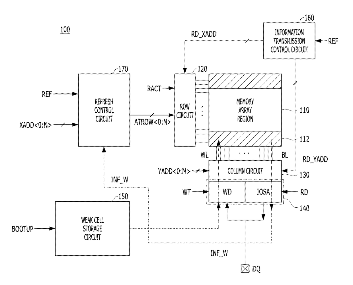
[0030]Various embodiments will be described below in more detail with reference to the accompanying drawings. The present invention may, however, be embodied in different forms and should not be construed as limited to the embodiments set forth herein. Rather, these embodiments are provided so that this disclosure will be thorough and complete, and will fully convey the scope of the present invention to those skilled in the art. Throughout the disclosure, like reference numerals refer to like parts throughout the various figures and embodiments of the present invention.

[0031]1 In general, after tests are performed through various methods for a weak cell, information on a detected weak cell hereinafter, referred to as a ‘weak cell information’, is stored in a nonvolatile memory such that the stored data may be retained even though power supply is cut off.

[0032]If the weak cell information stored in the nonvolatile memory is used in a normal operation by being immediately read out aft...


PUM


Abstract

A semiconductor memory device including a weak cell storage circuit suitable for programming therein weak cell information, and outputting the weak cell information in an initialization operation; a cell array region including a first cell region which stores the weak cell information received from the weak cell storage circuit, in the initialization operation; a refresh address generation block suitable for generating a refresh address by counting a refresh signal, and outputting a weak cell address corresponding to the weak cell information outputted from the first cell region, as the refresh address, with a predetermined cycle; and a refresh circuit suitable for performing a refresh operation for a word line corresponding to the refresh address, among a plurality of word lines.

Description

CROSS-REFERENCE TO RELATED APPLICATION[0001]This application claims priority under 35 U.S.C. §119 to Korean Patent Application No. 10-2016-0080146, filed on Jun. 27, 2016, the disclosure of which is herein incorporated by reference in its entirety.TECHNICAL FIELD[0002]Exemplary embodiments relate to a semiconductor design technology, and more particularly, to a semiconductor memory device which performs a refresh operation.DISCUSSION OF THE RELATED ART[0003]In general, a memory cell of a semiconductor memory device such as a dynamic random access memory (DRAM) is constructed by a transistor serving as a switch and a capacitor storing charges or data. Data is identified as ‘high’ (logic 1) or ‘low’ (logic 0) depending on whether charges are present in the capacitor of the memory cell, that is, whether the voltage of the terminal of the capacitor is high or low.[0004]In principle, storage of data does not consume power because the storage of data is implemented in such a manner that c...

Claims


Application Information

Patent Timeline
IPC IPC(8): G11C11/406G11C11/4072G11C11/4076G11C11/408
CPCG11C11/406G11C11/4076G11C11/4087G11C11/4072G11C11/40615G11C11/40622G11C2211/4061G11C11/408
Inventor KANG, KYEONG-PILCHI, SUNG-SOO
Owner SK HYNIX INC
Why Eureka
Try Eureka