
Vacuum reacting force welding method and device thereof

Active Publication Date: 2018-02-01
GUANGZHOU LEDTEEN OPTOELECTRONICS CO LTD
View PDF2 Cites 2 Cited by
  • Summary
  • Abstract
  • Description
  • Claims
  • Application Information

AI Technical Summary

Benefits of technology

The present invention provides a vacuum reacting force welding method that can apply an accelerating reacting force to the chip while lowering the voiding rate of the solder joints on the chip without causing damage. The method uses a linear motor for faster temperature increase and decrease, a vacuum to remove oxide film and dust particles, and pressure to assist in the welding process without causing damage to the chip. Compared to traditional methods, this invention can weld dozens of chips simultaneously, increasing production efficiency.

Problems solved by technology

Improper handling of these factors easily leads to a thick intermetallic compound (IMC) layer, an uneven distribution of the intermetallic compound layer and a higher voiding rate, which would cause a potential reliability problem.
There are following deficiencies in the above equipment and process thereof:(1) The infrared reflow furnace has the shortcomings of a slow heating / cooling rate, an uneven temperature zone and displacements of chips due to jitters in the transmission process.(2) The eutectic machine with nozzles and tweezers has a low output, and easily causes damage to chips, especially photoelectric chips, and thus affects the product performance.
Meanwhile, because of the eutectic chip by chip process, as to a multi-chip component, some eutectic chips which were performed eutectic first are subject to repeated heats, which leads to poor material performance of the chips.
It is suitable for larger chip packages while unsuitable for small chips and chips with fragile surfaces.

Method used


Image

  • Vacuum reacting force welding method and device thereof
  • Vacuum reacting force welding method and device thereof
  • Vacuum reacting force welding method and device thereof

Examples


Embodiment Construction

[0040]The invention will now be described further below with reference to attached drawings and specific embodiments thereof,

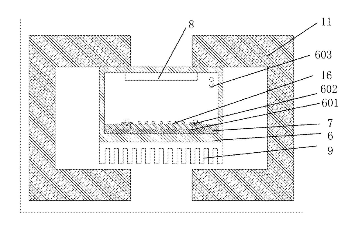
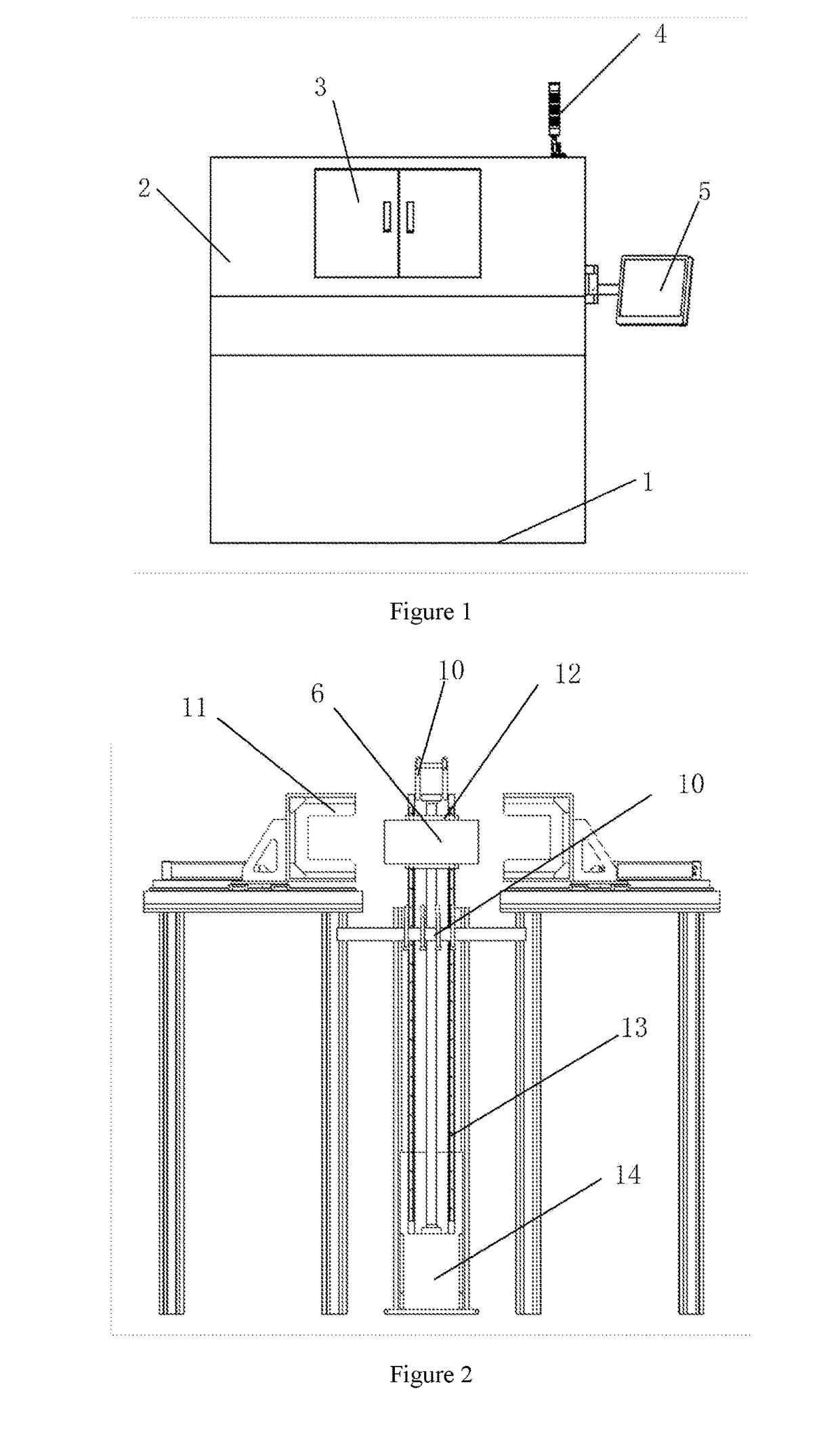
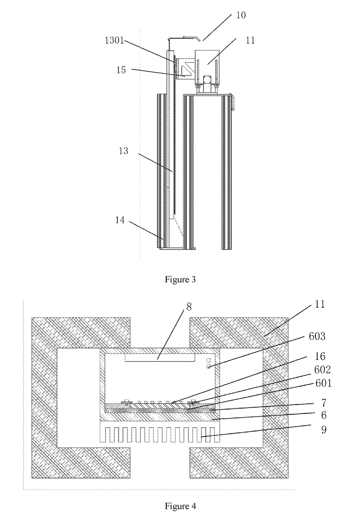
[0041]A vacuum reacting force welding method, comprising the following steps:[0042]S1. die-bonding a chip onto a substrate through solder to form a semi-finished product;[0043]S2. placing the semi-finished product into a vacuum eutectic cavity of a vacuum eutectic stove;[0044]S3. vacuum-pumping the vacuum eutectic cavity;[0045]S4. preheating the vacuum eutectic cavity to slowly increase the temperature;[0046]S5. heating the vacuum eutectic cavity quickly to melt the solder;[0047]S6. applying an acting force to the vacuum eutectic cavity to accelerate a rise of the vacuum eutectic cavity after the vacuum eutectic cavity descends;[0048]S7. performing forced refrigeration to the exterior of the vacuum eutectic cavity, while introducing a protective gas to the interior thereof;[0049]S8. releasing the vacuum state of the vacuum eutectic cavity after the solder is s...


PUM

PropertyMeasurementUnit
Temperatureaaaaaaaaaa
Forceaaaaaaaaaa
Accelerationaaaaaaaaaa

Abstract

The present invention discloses a vacuum reacting force welding method, comprising the following steps: die-bonding a chip onto a substrate through soldering to form a semi-finished product; placing the semi-finished product into a vacuum eutectic cavity (6) of a vacuum eutectic stove; vacuum-pumping the vacuum eutectic cavity; preheating the vacuum eutectic cavity to slowly increase the temperature; heating the vacuum eutectic cavity quickly to melt the solder; applying an acting force to the vacuum eutectic cavity to accelerate a rise of the vacuum eutectic cavity after the vacuum eutectic cavity descends; performing forced refrigeration to the exterior of the vacuum eutectic cavity, while introducing a protective gas to the interior thereof; releasing the vacuum state of the vacuum eutectic cavity after the solder is solidified. This invention also discloses a welding device using the vacuum reacting force eutectic welding method described herein.

Description

CROSS REFERENCE TO RELATED APPLICATIONS[0001]This application is the national phase entry of International Application No. PCT / CN2015 / 090464, filed on Sep. 23, 2015, the entire contents of which are incorporated herein by reference.TECHNICAL FIELD[0002]The invention relates to a vacuum eutectic welding device, specifically relates to a vacuum reacting force welding method and device thereof.BACKGROUND OF THE INVENTION[0003]Eutectic welding technology is widely applied in the field of microelectronics and optoelectronic packaging, such as the bonding of a chip and a substrate, bonding of the substrate and a housing, packaging a cover plate of the housing, etc. As a connection material of the devices, a solder joint is responsible for mechanical connections and electrical connections, heat exchanges, etc. Compared with the ordinary conductive adhesive bonding method, eutectic welding technology with the advantages of high thermal conductivity, small resistance, high reliability, etc.,...

Claims


Application Information

Patent Timeline
IPC IPC(8): H01L23/495B23K3/02B23K1/008
CPCH01L23/49513B23K1/008B23K3/023H01L2224/83805H01L2924/01322H01L24/75H01L2224/8309H01L2224/83097H01L2224/83098H01L2224/75102H01L24/00
Inventor SU, JIABING
Owner GUANGZHOU LEDTEEN OPTOELECTRONICS CO LTD
Learn More