Laser annealing method, laser annealing apparatus, and manufacturing process for thin film transistor

Active Publication Date: 2018-02-08
V TECH CO LTD
View PDF2 Cites 5 Cited by
  • Summary
  • Abstract
  • Description
  • Claims
  • Application Information

AI Technical Summary

Benefits of technology

The present invention provides a laser annealing method and apparatus, as well as a TFT manufacturing process, that can reduce leak current through a simplified process. The method involves multiple irradiations of the laser light with changing irradiation area on an amorphous silicon thin film to achieve a grain size distribution where crystal grain size is reduced from the central portion toward the side edge portion. This results in increased resistance to crystallization, ultimately reducing the leak current.

Problems solved by technology

In this case, since a polysilicon film is formed in regions below the source and drain electrodes as well, an electric field intensity is accordingly increased, making it difficult to reduce a so-called leak current (off current) generated when the TFT is turned off.
In order to deal with such a problem, an LDD (Lightly Doped Drain) structure, for example, is adopted, but it requires a complicated manufacturing process and is expensive.

Method used


Image

  • Laser annealing method, laser annealing apparatus, and manufacturing process for thin film transistor
  • Laser annealing method, laser annealing apparatus, and manufacturing process for thin film transistor
  • Laser annealing method, laser annealing apparatus, and manufacturing process for thin film transistor

Examples


Embodiment Construction

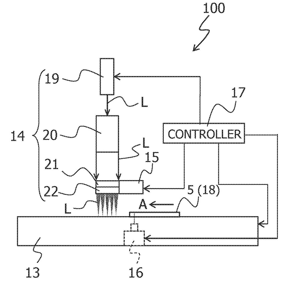
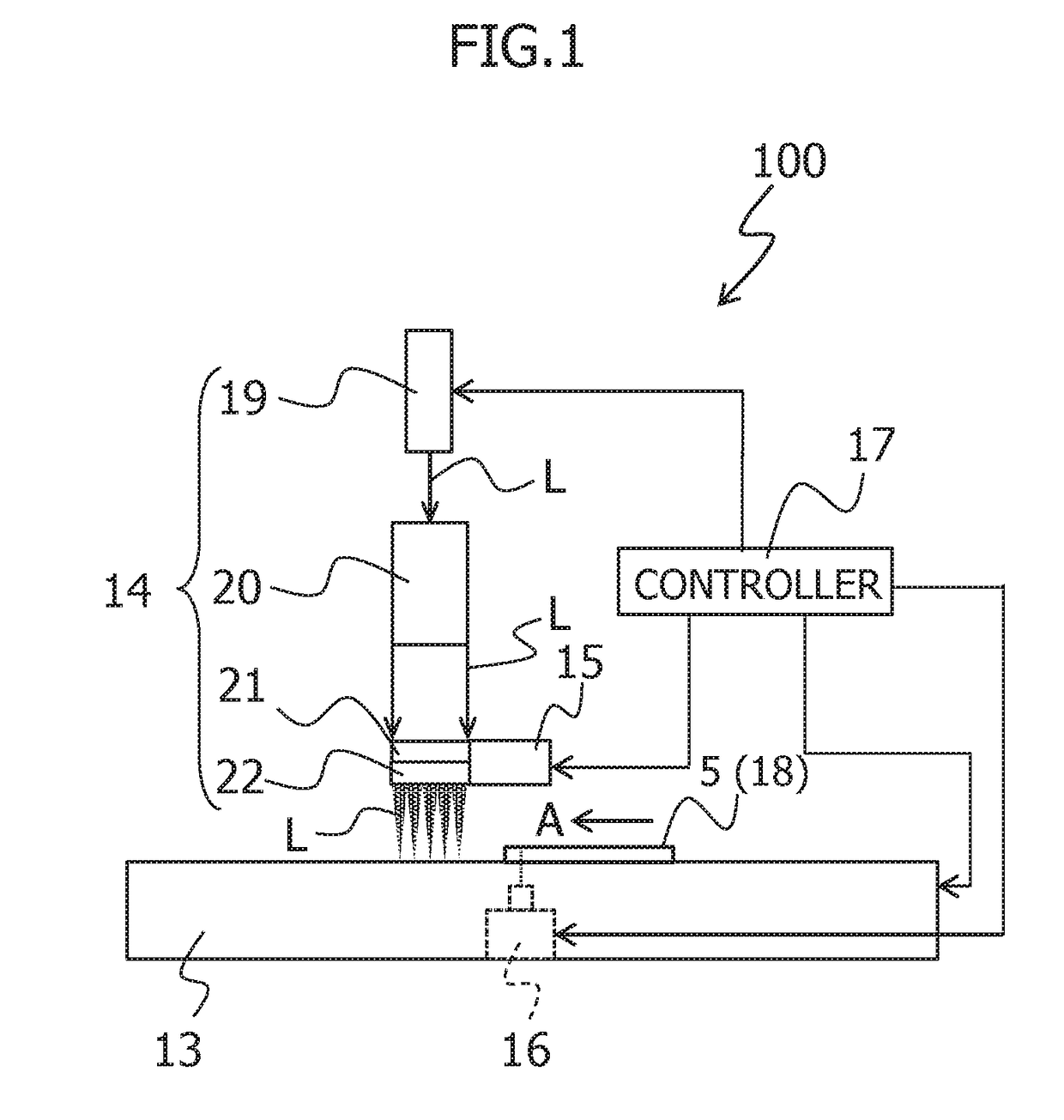
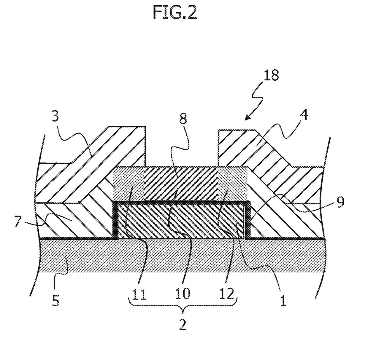
[0021]Embodiments of the present invention will be described below in detail with reference to the accompanying drawings. FIG. 1 is a schematic diagram showing an embodiment of a laser annealing apparatus of the present invention. FIG. 2 is a cross-sectional view showing an embodiment of a TFT manufactured by the laser annealing apparatus of the present invention. A laser annealing apparatus 100 of FIG. 1 performs laser annealing on an amorphous silicon thin film in a region corresponding to a gate electrode on a TFT substrate 5 to form a semiconductor layer of a TFT 18.

[0022]More specifically, the laser annealing apparatus 100 includes a conveyance means 13, a laser illumination optical system 14, an alignment means 15, an image capture means 16, and a controller 17. Note that the laser illumination optical system 14 is an example of an optical system, and the controller 17 is an example of a control means. Also, the TFT substrate 5 is an example of a substrate applicable in this e...


PUM


Abstract

The present invention provides a laser annealing method for irradiating laser light L to an amorphous silicon thin film deposited on a substrate to obtain polysilicon, the method including: multiply irradiating the laser light L while changing an irradiation area of the laser light L on the amorphous silicon thin film to achieve such a grain size distribution that a crystal grain size of the polysilicon decreases from a central portion to a side edge portion at least along a center line C of the irradiation area of the laser light L. The above laser annealing method can reduce a leak current through a simple process.

Description

CROSS-REFERENCE TO RELATED APPLICATIONS[0001]This application is a continuation application of PCT / JP2016 / 064345, filed on May 13, 2016, which claims priority to Japanese Patent Application No. 2015-102137, filed on May 19, 2015, all of which are hereby incorporated by reference in their entirety for all purposes.BACKGROUND OF THE INVENTION1. Field of the Invention[0002]The present invention relates to a laser annealing method for an amorphous silicon thin film, and more particularly, relates to a laser annealing method, a laser annealing apparatus, and a manufacturing process for a thin film transistor, which can reduce a leak current in the thin film transistor.2. Description of Related Art[0003]In general, thin film transistors (hereinafter referred to as “TFTs”) have a structure in which a gate electrode, a source electrode, a drain electrode, and a semiconductor layer are laminated. In such a structure, a TFT having a polysilicon thin film as the semiconductor layer excels in e...

Claims


Application Information

Patent Timeline
IPC IPC(8): H01L29/66H01L27/12H01L29/786H01L21/20
CPCH01L29/66757H01L21/2026H01L27/1285H01L29/78675H01L21/268H01L29/66765H01L29/78696H01L27/1229H01L21/02686H01L21/02678H01L21/02532H01L21/02595H01L21/02691H01L21/324H01L29/786H01L21/20
Inventor MIZUMURA, MICHINOBU
Owner V TECH CO LTD
Why Eureka
Try Eureka