Ion beam mill etch depth monitoring with nanometer-scale resolution

a technology of depth monitoring and nanometers, applied in the direction of instruments, semiconductor/solid-state device testing/measurement, superconductor devices, etc., can solve the problems of tedious and time-consuming parameter optimization procedures, little or no real-time feedback available during the actual etching process, etc., and achieve the effect of optimizing all operating parameters

Active Publication Date: 2018-02-22
RGT UNIV OF CALIFORNIA
View PDF6 Cites 5 Cited by
  • Summary
  • Abstract
  • Description
  • Claims
  • Application Information

AI Technical Summary

Benefits of technology

[0006]According to embodiments of the invention, a fixture and technique are provided to monitor the conductance of the material while it is being etched to obtain real-time feedback of the etching process, thus enabling the investigation of the material structure at nanoscale and allowing the optimization of all the operating parameters in a single run. For homogeneous materials with uniform conductivity, conductance scales linearly with thickness, making it possible to determine the real-time etch rate for optimization of the ion beam parameters such as pressure, beam voltage, current and neutralization. For materials with a well-known etch rate, the inventive technique can be used to probe changes in conductivity as a function of depth into the material. For multilayer thin films, this method allows etching to be stopped precisely at the transition between two layers by detecting the difference in conductivity.

Problems solved by technology

Unfortunately, the procedures for parameter optimization can be tedious and time-consuming.
In addition, there is little or no real-time feedback available for monitoring during the actual etching process.

Method used


Image

  • Ion beam mill etch depth monitoring with nanometer-scale resolution
  • Ion beam mill etch depth monitoring with nanometer-scale resolution
  • Ion beam mill etch depth monitoring with nanometer-scale resolution

Examples


Embodiment Construction

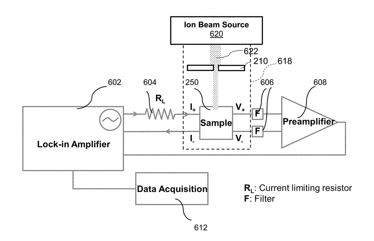
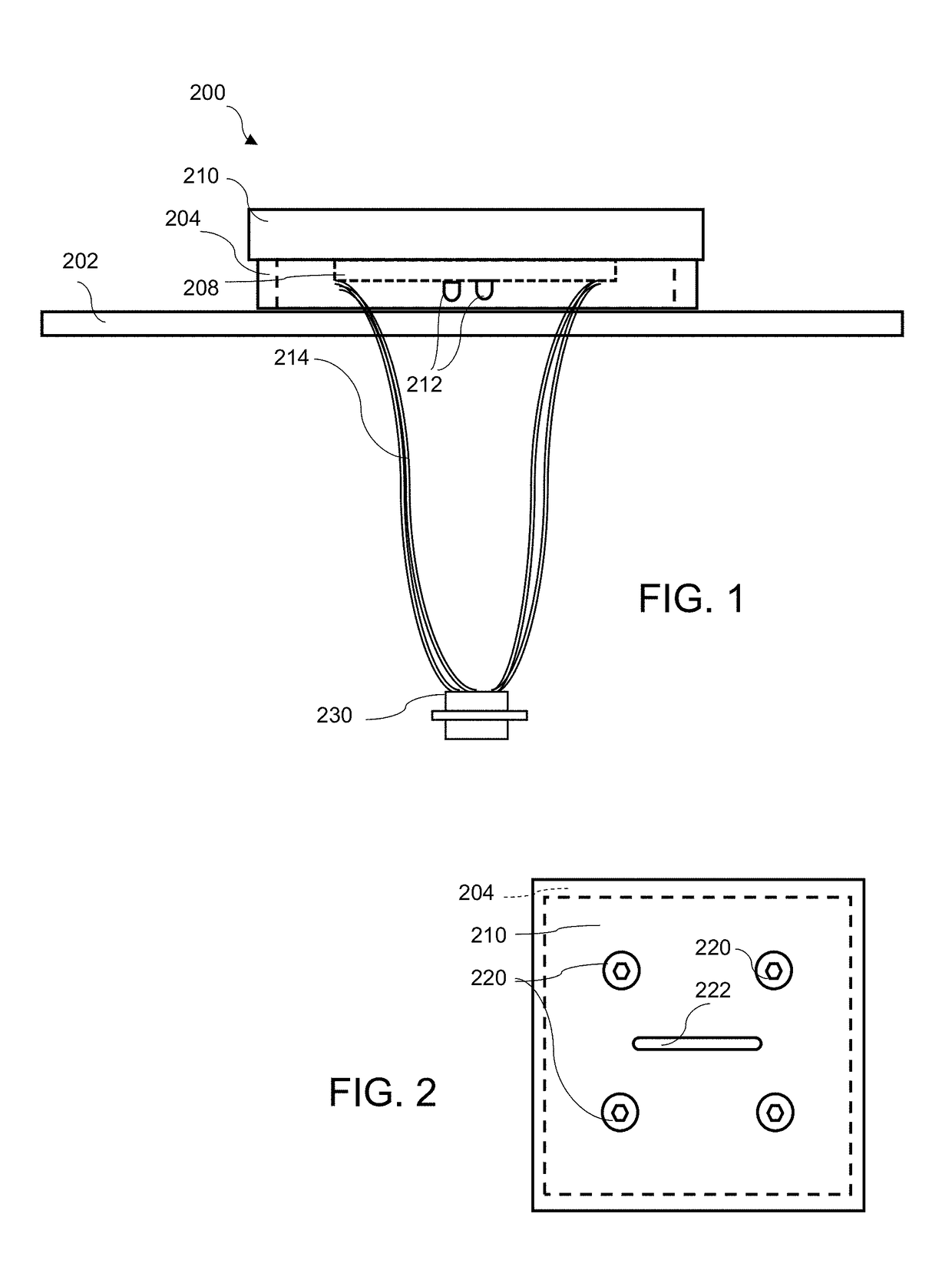
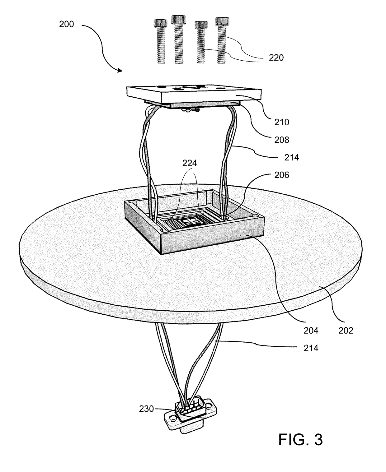
[0024]An assembly and method are provided for measurement of the conductance of a sample in the hostile environment of a broad beam ion source. The inventive fixture shields the electrical contacts and wires of the assembly from being etched in the beam and masks the electrodes any re-deposited material that could short-circuit the measurement. The materials used to construct the fixture are selected to tolerate high temperatures and thermal variations, as well as to be chemically compatible with the gases used in the etch process. The examples described herein focus on the milling of oxides and noble metals with inert argon, and therefore are less concerned with potentially adverse chemical reactions that could occur with harsh etch gases. Those of skill in the art will be capable of selecting materials appropriate to withstand the intended etch conditions.

[0025]As used herein, “etching / milling” means a process in which ions are accelerated toward a target surface to bombard the ma...


PUM

PropertyMeasurementUnit
thickaaaaaaaaaa
thickaaaaaaaaaa
currentaaaaaaaaaa

Abstract

A method for measuring conductance of a material real-time during etching/milling includes providing a fixture having a socket for receiving the material. The socket is attached to a printed circuit board (PCB) mounted on one side of a plate that has at least one opening for providing ion beam access to the material sample. Conductive probes extend from the other side of the PCB to contact and span a target area of the material. A measurement circuit in electrical communication with the probes measures the voltage produced when a current is applied across the material sample to measure changes in electrical properties of the sample over time.

Description

RELATED APPLICATIONS[0001]This application claims the benefit of the priority of provisional Application No. 62 / 377,504, filed Aug. 19, 2016, which is incorporated herein by reference in its entirety.GOVERNMENT RIGHTS[0002]This invention was made with government support under Contract No. DEACO2 05CH11231 from the Basic Energy Sciences (BES) program of the U.S. Department of Energy (DOE) and Grant No. FA9550-07-1-0493 from the Air Force Office of Scientific Research (AFOSR). The government has certain rights in the invention.FIELD OF THE INVENTION[0003]The present invention relates to ion etching of nanoscale features and more specifically to a fixture and method for ion etching with real-time feedback to obtain precise control of etch parameters.BACKGROUND[0004]Broad beam ion sources were originally developed by the United States National Aeronautics and Space Administration (NASA), as well as by other countries, for electric space-propulsion programs in the 1960's. These broad bea...

Claims


Application Information

Patent Timeline
Patent Type & Authority Applications(United States)
IPC IPC(8): H01J37/30H01J37/304G01N27/04G01B7/06
CPCH01J37/3005H01J37/304G01N27/041G01B7/06H01L39/249H01L22/26H01L39/2496H01J37/3053G01B7/26H01J37/3056H01J2237/3174H01J2237/30466H01J2237/30455H01J2237/08H10N60/0884H10N60/0941
Inventor CYBART, SHANE A.DYNES, ROBERT C.
Owner RGT UNIV OF CALIFORNIA
Why Eureka
Try Eureka