Ceramic electronic component and mounting structure of the same

a technology of ceramic electronic components and mounting structures, which is applied in the direction of fixed capacitor details, sustainable manufacturing/processing, final product manufacturing, etc., can solve the problems of circuit failure, failure to function, and failure to meet the requirements of the current fuse,

Active Publication Date: 2018-03-22
MURATA MFG CO LTD
View PDF12 Cites 2 Cited by
  • Summary
  • Abstract
  • Description
  • Claims
  • Application Information

AI Technical Summary

Benefits of technology

[0100]Hereinafter, in order to confirm advantageous effects and features of the preferred embodiments of the present invention, experimental examples will be described. FIG. 12 is a circuit diagram of an experimental example 1, an experimental example 2, and a comparative experimental example 1 that confirm the advantageous effects and features of the ceramic electronic components according to the preferred embodiments of the present invention, and a case where two ceramic electronic components connected in series to span across PN of DC line are included. The two capacitors in the center in the diagram connected in series are ceramic electronic components (multilayer ceramic capacitors) to be tested. DC voltage is applied to the multilayer ceramic capacitors to be tested from a circuit connected on the left side, and ripple voltage is applied to the multilayer ceramic capacitors to be tested from a circuit connected on the right side. FIG. 13 is a circuit diagram of an experimental example 3 that confirms the effects and features of the ceramic electronic components according to the preferred embodiments of the present invention, an LC resonance load is applied to the multilayer ceramic capacitor to be tested located on upper right in the diagram. DC voltage is applied to the multilayer ceramic capacitor to be tested by a circuit connected on the left side, and ripple voltage is applied to the multilayer ceramic capacitor to be tested from a circuit connected on the right side.
and features of the preferred embodiments of the present invention, experimental examples will be described. FIG. 12 is a circuit diagram of an experimental

Problems solved by technology

As a result, there are risks that the ceramic electronic component itself, a battery and a conductor connected to the short circuit in the electronic apparatus, or the like will generate abnormal heat, and smoking and fire will occur.
However, in such a case, there are a problem that the circuit does not function due to the current fuse functioning and a problem in reliability with respect to the current fuse.
However, when one multilayer ceramic capacitor fails actually in such a circuit, and a short-circuit path is formed therein, there are risks that the faulty multilayer ceramic capacitor will generate abnormal heat, a mounting substrate and combustibles in the periphery will burn, and smoking and fire will arise, depending on the state of the failure and a ripple current flowing in the multilayer ceramic capacitor.
However, because such a current fuse does not function when only one multilayer ceramic capacitor fails, for example, the above-described abnormal heat generation or the like cannot be avoided in the same manner.
Additionally, in an LC resonance circuit as illustrated in FIG. 14C, when only an AC load with a frequency which makes impedance of a multilayer ceramic capacitor sufficiently small is applied, impedance of the multilayer ceramic capacitor with a short-circuit path formed therein does not become sufficiently small in comparison with impedance of a multilayer ceramic capacitor component.
However, there are risks that the faulty multilayer ceramic capacitor will generate abnormal heat by an AC current flowing therein, a mounting substrate and combustibles in the periphery will burn, and smoking and fire will arise.
For example, deterioration or failure such as to cause heat generation more than expected by simple increase in loss may also arise.
However, because a current fuse cannot cope with such failure of course, smoking and fire, or the like as described above cannot be avoided.
However, because the temperature fuse cannot directly detect temperature of a ceramic electronic component, the temperature fuse takes time until it operates.
As a result, smoking and fire by the abnormal heat generation as described above cannot be avoided.
Furthermore, using the ceramic electronic component in which the heat generation at the failure is expected together with the current fuse as described above may make a circuit design or assembly difficult.
Additionally, this causes increase in ESR or ESL of the circuit, prevents a performance of the ceramic electronic component in the circuit from exerting, and thus is not realistic.
Additionally, a current path is complicated in the ceramic electronic component, which causes an increase in ESL and deterioration in high-frequency characteristics, an increase in ESR and an increase in heat generation and loss, and furthermore, a decrease in an allowable current.
In other words, there are problems that the ceramic electronic component in Japanese Unexamined Patent Application Publication No. 11-54357 has low performance in comparison with an electronic component without a fuse function, and has completely insufficient performance depending on an incorporated circuit.

Method used


Image

  • Ceramic electronic component and mounting structure of the same
  • Ceramic electronic component and mounting structure of the same
  • Ceramic electronic component and mounting structure of the same

Examples


experimental example 1

[0101]In the experimental example 1, a circuit with multilayer ceramic capacitors as the ceramic electronic components according to the preferred embodiments of the present invention connected in series, as shown in FIG. 12, was manufactured, a fail-safe function of the multilayer ceramic capacitors were evaluated. One of the two multilayer ceramic capacitors connected in series was mounted on the substrate, after being subjected to dielectric breakdown by a dielectric breakdown voltage testing machine, in order to reproduce a failure state. Additionally, the capacitor connected on the right side in the circuit in FIG. 12 included a breakdown voltage of about 2 kV, and electrostatic capacitance of about 500 μF.

working example 1

[0102]In accordance with the manufacturing method described above, a sample (multilayer ceramic capacitor) for a working example 1 was manufactured. Specifications of the working example 1 and a fixing method between the substrate connection terminal and the mounting substrate were as follows.

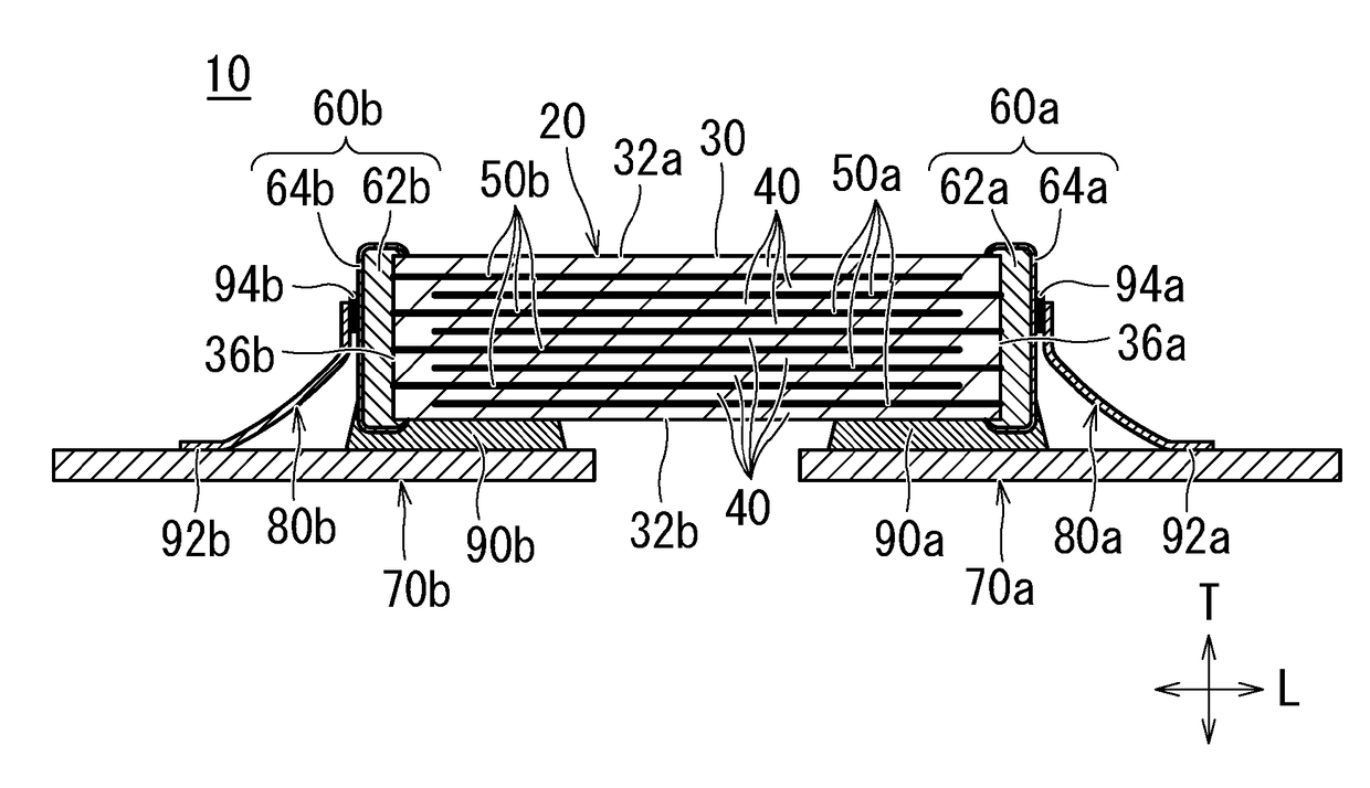
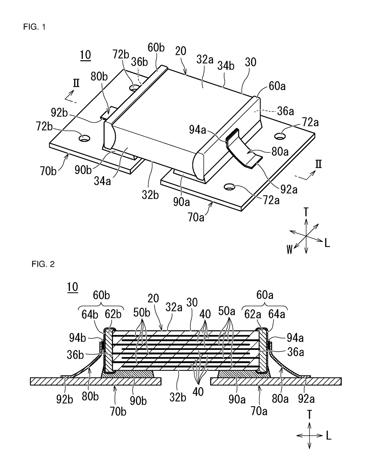
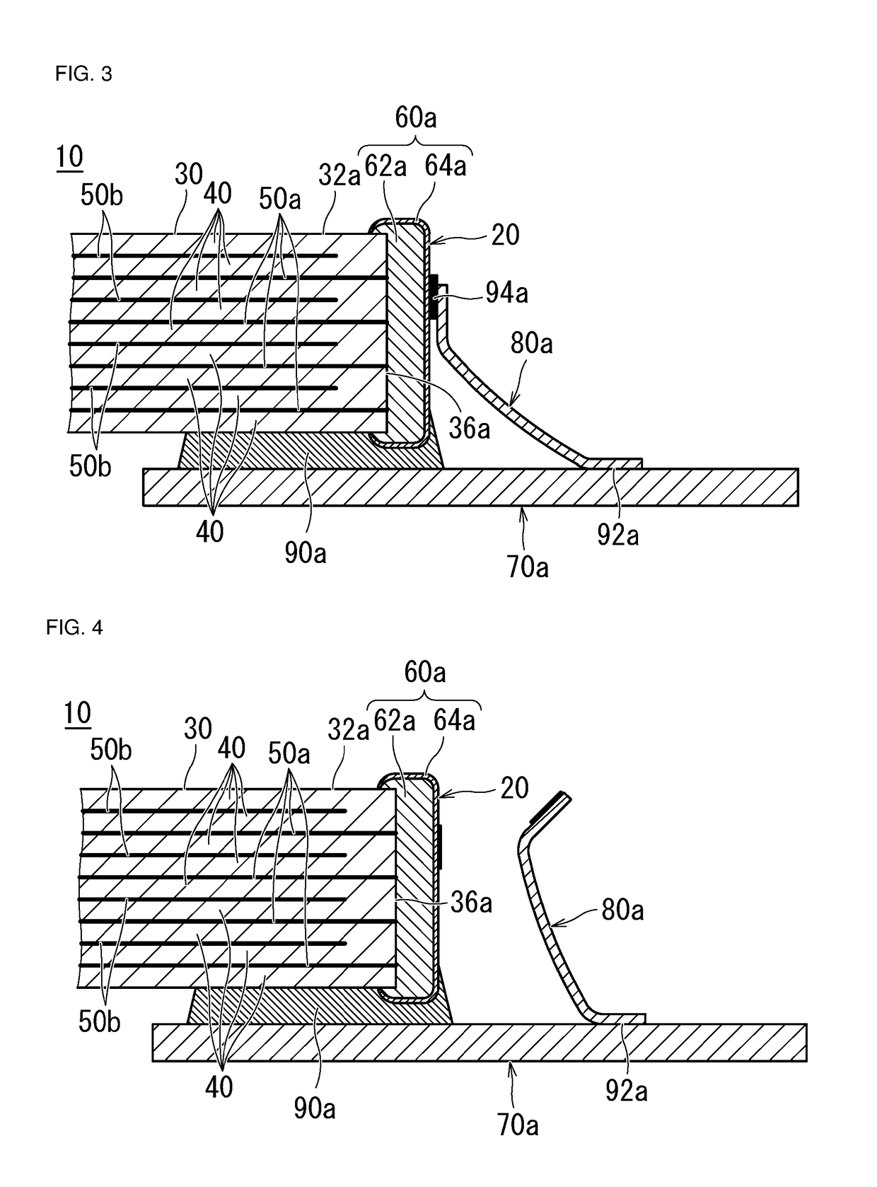
[0103]Chip size (L×W×T): 16 mm×20 mm×3.7 mm (design value)

[0104]Ceramic layer: BaTiO3

[0105]Inner electrode layer: Ni

[0106]Structure of outer electrode[0107]Base electrode layer: Cu[0108]Plating layer: none

[0109]Structure of metal terminal[0110]C7035TM04 made by DOWA OLIN[0111]Quantity: 2 in total (only one pair)[0112]Shape of end portion on substrate connection terminal side (the second end portion): substantially Y shape[0113]Thickness: 0.1 mm

[0114]Bonding material bonding outer electrode and metal terminal: M705 made by Senju Metal Industry

[0115]Bonding material bonding outer electrode and substrate connection terminal: silicone based adhesive KE-1830 made by Shin-Etsu Silicone

[0116]Bonding ...

experimental example 2

[0143]In accordance with the manufacturing method described above with respect to the preferred embodiments of the present invention, a sample (multilayer ceramic capacitor) for a working example 2 was manufactured. The working example 2 included the same or a similar structure as that of the working example 1 excluding the substrate connection terminal being not included. Additionally, the second end portion of the metal terminal was directly connected to the land portion of the mounting substrate. Specifications of the working example 2 were as follows.

[0144]Chip size (L×W×T): 16 mm×20 mm×3.7 mm (design value)

[0145]Ceramic layer: BaTiO3

[0146]Inner electrode layer: Ni

[0147]Structure of outer electrode[0148]Base electrode layer: Cu[0149]Plating layer: none

[0150]Structure of metal terminal[0151]C7035TM04 made by DOWA OLIN[0152]Quantity: two in total (only one pair)[0153]Shape of end portion on mounting substrate side (the second end portion): substantially Y shape[0154]Thickness: 0....


PUM

PropertyMeasurementUnit
thicknessaaaaaaaaaa
thicknessaaaaaaaaaa
thicknessaaaaaaaaaa

Abstract

A ceramic electronic component includes a multilayer body, an electronic component main body including first and second outer electrodes on the surface of multilayer body, a first substrate connection terminal bonded to at least one of the first outer electrode and the multilayer body by a bonding material that is electrically insulating, and a first metal terminal electrically connecting the first outer electrode and the first substrate connection terminal, in which, while the first metal terminal maintains an elastically deformed state, a first end portion thereof is bonded to the first outer electrode by an electrically conductive bonding material, and a second end portion thereof is bonded to the first substrate connection terminal by a bonding section with a different melting point from that of the bonding material.

Description

CROSS REFERENCE TO RELATED APPLICATIONS[0001]This application claims the benefit of priority to Japanese Patent Application No. 2016-184699 filed on Sep. 21, 2016. The entire contents of this application are hereby incorporated herein by reference.BACKGROUND OF THE INVENTION1. Field of the Invention[0002]The present invention relates to a ceramic electronic component and a mounting structure thereof.2. Description of the Related Art[0003]When a short-circuit path is formed in a ceramic electronic component due to failure, a short circuit is formed in an electronic apparatus in which the ceramic electronic component is incorporated, and a current not less than a rated current (hereinafter, referred to simply as “overcurrent”) flows in the electronic apparatus in some cases. As a result, there are risks that the ceramic electronic component itself, a battery and a conductor connected to the short circuit in the electronic apparatus, or the like will generate abnormal heat, and smoking...

Claims


Application Information

Patent Timeline
Patent Type & Authority Applications(United States)
IPC IPC(8): H01G4/232H01G4/012H01G4/002H01G4/008H01G4/33H01G4/258
CPCH01G4/232H01G4/012H01G4/002H01G4/008H01G4/33H01G4/258H01G4/248H01G4/1227H01G4/1236H01G4/30H01G4/12H01G4/2325H05K1/111H05K3/305H05K3/3442H05K2201/10015H05K2201/1028H05K2201/10409H05K2201/10636H05K2201/10916H05K2201/10946H05K2201/10962H01G2/06Y02P70/50H01G2/04
Inventor AKIYOSHI, TEPPEI
Owner MURATA MFG CO LTD
Why Eureka
Try Eureka