SiC WAFER PRODUCING METHOD

Active Publication Date: 2018-03-29
DISCO CORP
View PDF3 Cites 18 Cited by
  • Summary
  • Abstract
  • Description
  • Claims
  • Application Information

AI Technical Summary

Benefits of technology

The present invention provides a method of producing SiC wafers with improved productivity. The method involves forming a modified layer in the SiC ingot, which has cracks propagating from it in opposite directions along the c-plane. The modified layer is then removed, resulting in a separation surface in the SiC ingot. The SiC ingot is then separated along this surface to produce a SiC wafer with the desired thickness. The method also includes chamfering the outer circumference of the SiC wafer to remove any burrs that could affect the grinding step, resulting in improved processing quality and stable processing quality.

Problems solved by technology

However, in producing the SiC wafer from the SiC ingot by using the prior art technique disclosed in Japanese Patent Laid-open No. 2013-49161, there is a problem such that the modified layers must be densely formed with a pitch of approximately 10 μm, causing a reduction in productivity.

Method used


Image

  • SiC WAFER PRODUCING METHOD
  • SiC WAFER PRODUCING METHOD
  • SiC WAFER PRODUCING METHOD

Examples


Embodiment Construction

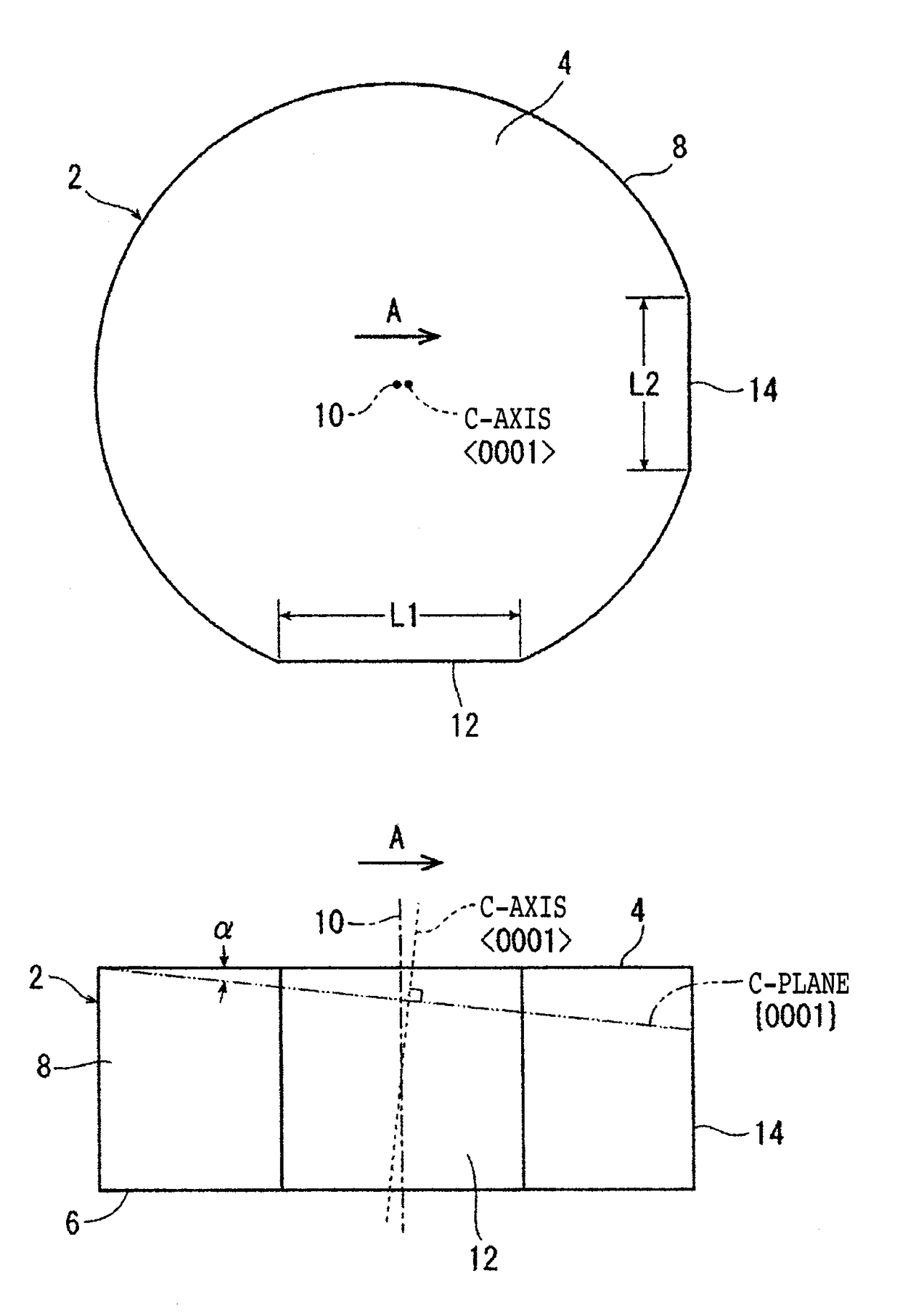
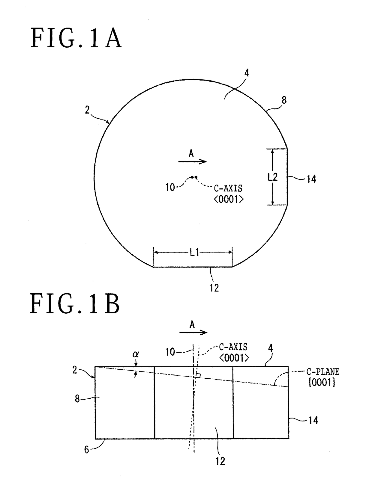
[0024]A preferred embodiment of the SiC wafer producing method according to the present invention will now be described with reference to the drawings. FIGS. 1A and 1B depict a generally cylindrical hexagonal single crystal SiC ingot 2 (which will be hereinafter referred to simply as “ingot 2”) as a workpiece to be processed. The ingot 2 has a substantially circular first surface 4, a substantially circular second surface 6 opposite to the first surface 4, a substantially cylindrical surface 8 formed so as to connect the first surface 4 and the second surface 6, a c-axis ( direction) extending from the first surface 4 to the second surface 6, and a c-plane ({0001} plane) perpendicular to the c-axis. In the ingot 2, the c-axis is inclined by an off angle α with respect to a normal 10 to the first surface 4. The off angle α (e.g., α=4°) is formed between the c-plane and the first surface 4 (the direction of formation of the off angle α is depicted by an arrow A in FIGS. 1A and 1B). Fu...


PUM


Abstract

A SiC wafer is produced from a single crystal SiC ingot. A modified layer is formed by setting a focal point of a pulsed laser beam inside the ingot at a predetermined depth from the upper surface of the ingot, the predetermined depth corresponding to the thickness of the wafer to be produced. The pulsed laser beam is applied to the ingot while moving the ingot in a first direction perpendicular to a second direction where an off angle is formed, thereby forming a modified layer in the first direction inside the ingot and cracks propagating from the modified layer along a c-plane. A separation surface is formed by indexing the ingot in the second direction and applying the laser beam plural times to thereby form a separation surface inside the ingot. Part of the ingot is separated along the separation surface to thereby produce the wafer.

Description

BACKGROUND OF THE INVENTIONField of the Invention[0001]The present invention relates to an SiC wafer producing method for producing an SiC wafer from a single crystal SiC ingot.Description of the Related Art[0002]Various devices such as integrated circuits (ICs), large-scale integrations (LSIs), and light-emitting diodes (LEDs) are formed by forming a functional layer on the front side of a wafer formed of Si (silicon) or Al2O3 (sapphire) and partitioning this functional layer into a plurality of separate regions along a plurality of division lines. Further, power devices or optical devices such as LEDs are formed by forming a functional layer on the front side of a wafer formed of single crystal SiC (silicon carbide) and partitioning this functional layer into a plurality of separate regions along a plurality of division lines. The division lines of such a wafer having these devices are processed by a processing apparatus such as a cutting apparatus and a laser processing apparatus...

Claims


Application Information

Patent Timeline
IPC IPC(8): B23K26/00B23K26/06B23K26/40B23K26/38
CPCB23K26/0057B23K26/0626B23K26/40B23K26/38B23K2203/56B23K26/402B23K26/53B23K2103/56B23K26/0853B23K26/0006B23K26/0622B23K2101/40H01L21/0201H01L21/02005B23K26/0823H01L21/02378H01L21/02433H01L21/02027H01L21/02021H01L21/02013H01L21/78
Inventor HIRATA, KAZUYA
Owner DISCO CORP
Why Eureka
Try Eureka