Memory control circuit and memory controlling method

Active Publication Date: 2018-03-29
SONY CORP
View PDF4 Cites 0 Cited by
  • Summary
  • Abstract
  • Description
  • Claims
  • Application Information

AI Technical Summary

Benefits of technology

[0004]There are cases where a DRAM becomes a noise source, and an influence of electromagnetic noise that an electric circuit close thereto receives becomes an issue as described above. One example is a sensor module. A sensor is demanded to be high in detection accuracy. It is expected that the use in which the sensor is close to the DRAM will be increased in future due to an increase in volume of data that the sensor outputs. As a method of reducing

Problems solved by technology

There are cases where a DRAM becomes a noise source, and an influence of electromagnetic

Method used


Image

  • Memory control circuit and memory controlling method
  • Memory control circuit and memory controlling method
  • Memory control circuit and memory controlling method

Examples


Embodiment Construction

[0015]In the following, embodiments of the disclosure will be described in detail with reference to the drawings. Incidentally, description will be made in the following order.

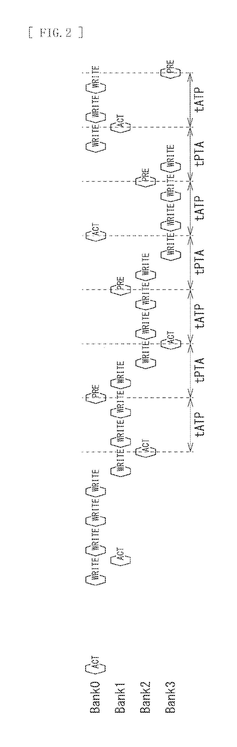
[0016]1. Memory Bus System including Memory Control Circuit[0017]1.1 Configuration (FIG. 1)[0018]1.2 Operation (FIG. 2 and FIG. 3)[0019]1.3 Modification (FIG. 4)[0020]1.4 Effects

[0021]2. Other Embodiments

1. Memory Bus System Including Memory Control Circuit

[0022][1.1 Configuration]

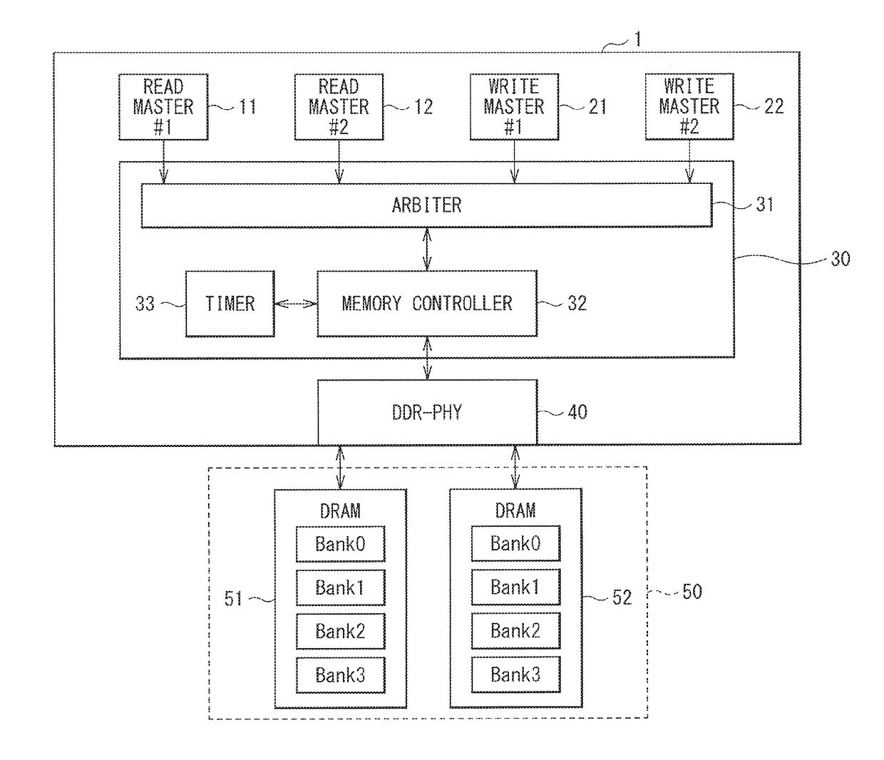
[0023]FIG. 1 illustrates one configuration example of a memory bus system including a memory control circuit according to one embodiment of the disclosure.

[0024]A memory bus system 1 is provided with one or more bus masters, a memory control unit 30, and a DDR-PHY (physical interface) 40. The bus masters are configured by, for example, a plurality of READ masters 11 and 12, and a plurality of WRITE masters 21 and 22. The memory control unit 30 has an arbiter 31, a memory controller 32, and a timer 33.

[0025]Although FIG. 1 illustrates...


PUM


Abstract

A memory control circuit of the disclosure includes a memory control unit that controls a timing of command issuance to cause (tATP+tPTA) to be constant, where, in a memory having a plurality of banks, tATP is a period from issuance of a first ACT command to issuance of a PRE command that is directed a bank same as or different from a bank to which the first ACT command is issued, and tPTA is a period from the issuance of the PRE command to issuance of a second ACT command that is directed to a bank same as or different from the bank to which the PRE command is issued.

Description

TECHNICAL FIELD[0001]The disclosure relates to a memory control circuit and a memory controlling method that are suitable for a DRAM (Dynamic Random Access Memory).BACKGROUND ART[0002]In an electronic apparatus mounted with a DRAM, there are cases where noise generated by the DRAM exerts an influence on the performance of the electronic apparatus. Various techniques are disclosed that are directed to a reduction of the influence of such noise. For example, Patent Literature 1 discloses a semiconductor storage device that has a plurality of DRAM memory sections and in which timings of refreshing operations are shifted from one another in the respective DRAM memory sections. In the semiconductor storage device, suppression is achieved of power supply noise caused by the refreshing operation, by shifting the timings of the refreshing operations from one another.CITATION LISTPatent Literature[0003]Patent Literature 1: Japanese Unexamined Patent Application Publication No. 2011-28790SUMM...

Claims


Application Information

Patent Timeline
IPC IPC(8): G06F3/06G06F12/02G11C7/22
CPCG06F3/0659G06F12/02G11C7/22G11C11/40615G11C8/12G11C11/40603G11C11/40618G11C11/4076G06F13/4234G06F13/16
Inventor IKARASHI, TAKAHIRO
Owner SONY CORP
Why Eureka
Try Eureka