Substrate for power module, collective substrate for power modules, and method for manufacturing substrate for power module

a technology for power modules and substrates, applied in the direction of ceramic layered products, chemistry apparatus and processes, other domestic articles, etc., can solve the problems of reducing the productivity of final products, generating more heat, and consuming more power of recent power semiconductor devices, so as to reduce the cost of ceramic plates formed from aluminum nitride, the effect of efficient mounting

Active Publication Date: 2018-04-12
SUMITOMO METAL SMI ELECTRONICS DEVICES +1
View PDF0 Cites 8 Cited by
  • Summary
  • Abstract
  • Description
  • Claims
  • Application Information

AI Technical Summary

Benefits of technology

[0027]For the first copper circuit plate having the third portion, the bond that can overflow from the first portion when a semiconductor device is joined to the first portion with a bond is blocked by the step formed between the second portion and the third portion. This prevents a short circuit between the first copper circuit plate and the second copper circuit plate.
[0028]The collective substrate for power modules according to the fourth aspect of the present invention includes first portions that are arranged regularly for mounting semiconductor devices. This allows semiconductor devices to be efficiently mounted onto the first portions.
[0029]The collective substrate for power modules according to the fourth aspect of the present invention increases the productivity of the final products.
[0030]The method for manufacturing a substrate for a power module according to the fifth aspect of the present invention is a method for manufacturing the power module substrate according to the first aspect of the present invention and the power module substrate according to the fourth aspect of the present invention. The method according to the fifth aspect enables manufacture of the power module substrate that promptly dissipates heat generated from the semiconductor device, and reduces heat stress at the joint interface between the ceramic plate and the copper plate resulting from the different thermal expansion coefficients of ceramics and copper to avoid separation of the edges of the copper circuit plate from the ceramic plate and cracks in the ceramic plate in the resultant power module substrate.
[0031]The method for manufacturing a substrate for a power module according to the fifth aspect of the present invention uses an inkjet method to form the second etching resist film. The resultant second etching resist film can have a cross-section in correspondence with any protrusions and recesses formed on the large copper plate surface. In other words, the second etching resist film can be formed at intended positions with high accuracy on the large copper plate with surface protrusions and recesses. This method easily forms the second etching resist film without rupture or breaks on any surface protrusions and recesses of the large copper plate. The subsequent etching thus forms precise protrusions and recesses on the large copper plate.
[0032]The method for manufacturing a substrate for a power module according to the sixth aspect of the present invention uses an inkjet method to form the fourth etching resist film. The resultant fourth etching resist film can have a cross-section in correspondence with any protrusions and recesses formed on the large copper plate surface. In other words, the fourth etching resist film can be formed at intended positions with high accuracy on the large copper plate with surface protrusions and recesses. The method forms the fourth etching resist film without rupture or breaks on any surface protrusions and recesses of the large copper plate. The subsequent etching thus forms precise protrusions and recesses on the large copper plate.

Problems solved by technology

Recent power semiconductor devices consume more power, and generate more heat.
However, the power module substrate including the joined structure of the ceramic plate and the copper plate can have issues including lower heat dissipation through the ceramic plate with low heat conductivity, and separation of the edges of the copper plate from the ceramic plate or cracks in the ceramic plate under heat stress at the joint interface between the ceramic plate and the copper plates resulting from the different thermal expansion coefficients of ceramics and copper.
However, the ceramic plate formed from aluminum nitride is very expensive.
However, the thinner ceramic plate formed from an alumina-based ceramic can have a lower strength.
However, the ceramic plate formed from silicon nitride is very expensive.
However, the increased heat stress at the joint interface between the ceramic plate and the copper plates resulting from the different thermal expansion coefficients of ceramics and copper may cause separation of the edges of the copper plate and cracks in the ceramic plate.
However, the active metal brazing material layer can slightly degrade heat dissipation.
The power module substrate prepared by the DCB using heat includes the copper plates and the ceramic plate joined either directly, or with a very thin copper oxide layer between them, and thus has high heat transfer, or high heat dissipation, at the interfaces between the ceramic plate and the copper plates.
However, the ceramic plate or the copper plates still need some measures to reduce stress at the joint interfaces between the ceramic plate and the copper plate edges.

Method used


Image

  • Substrate for power module, collective substrate for power modules, and method for manufacturing substrate for power module
  • Substrate for power module, collective substrate for power modules, and method for manufacturing substrate for power module
  • Substrate for power module, collective substrate for power modules, and method for manufacturing substrate for power module

Examples


Embodiment Construction

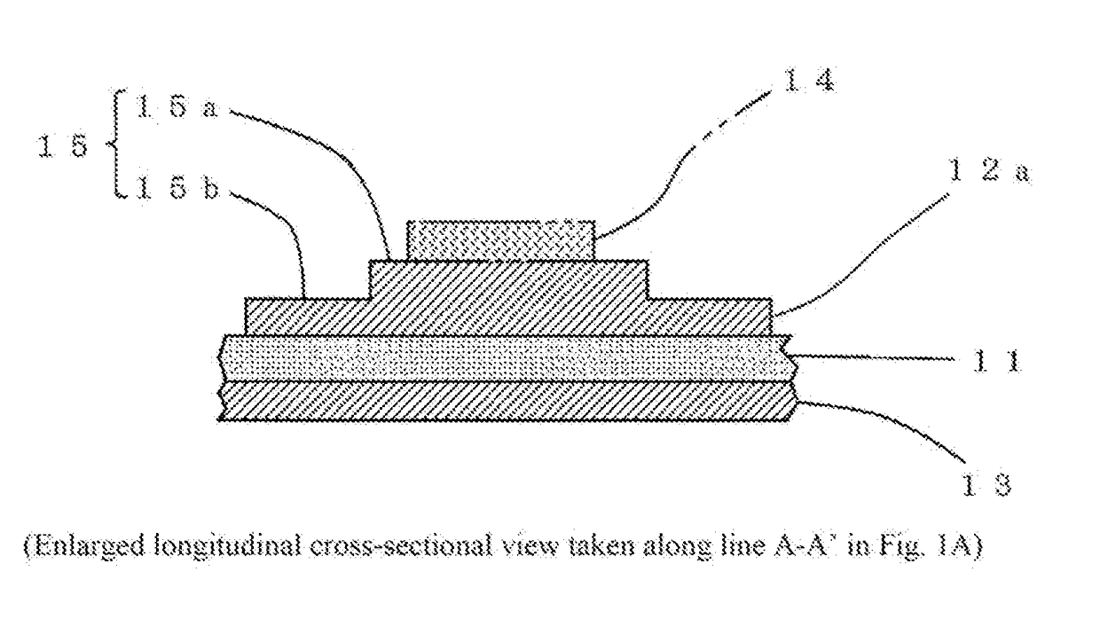
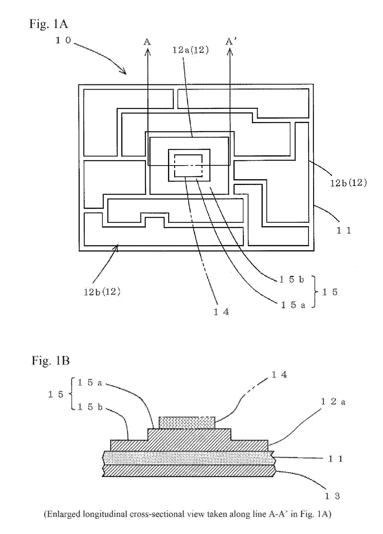
[0040]A substrate for a power module according to one embodiment of the present invention will now be described with reference to FIGS. 1A and 1B.

[0041]As shown in FIGS. 1A and 1B, a substrate 10 for a power module according to the present embodiment includes a ceramic plate 11, and an island-shaped copper circuit plate 12, which is joined to one main surface of the ceramic plate 11. The entire copper circuit plate 12 forms an electric circuit. The power module substrate 10 further includes a heat dissipation copper plate 13, which is joined to the other main surface of the ceramic plate 11 to cover the entire surface of the other main surface (where the term entire includes substantially entire). The heat dissipation copper plate 13 dissipates heat generated from an electronic component (e.g., a semiconductor device 14) mounted on the copper circuit plate 12 downward (toward the other main surface).

[0042]The copper circuit plate 12 includes a first copper circuit plate 12a for moun...


PUM

PropertyMeasurementUnit
temperatureaaaaaaaaaa
thicknessaaaaaaaaaa

Abstract

A power module substrate allows prompt heat dissipation from a semiconductor device and avoids separation of a ceramic plate and a copper plate at their joint interface and cracks in the ceramic plate. A power module substrate for mounting a semiconductor device includes a ceramic plate, a copper circuit plate on a main surface of the ceramic plate, and a heat dissipation copper plate on a surface of the ceramic plate opposite to the main surface. The copper circuit plate includes at least one first copper circuit plate and at least one second copper circuit plate different from the first circuit board. The first copper circuit plate includes a first portion on which the semiconductor device is mountable, and a second portion outward from the first portion and surrounding the first portion and thinner than the first portion.

Description

CROSS-REFERENCE TO RELATED APPLICATIONS[0001]This application is a continuation application of International Patent Application No. PCT / JP2016 / 065838 filed on May 27, 2016, which claims priority to Japanese Patent Application No. 2015-107141 filed on May 27, 2015, the entire contents of which are incorporated by reference.BACKGROUND OF INVENTIONField of the Invention[0002]The present invention relates to a power module substrate, including a ceramic plate and a copper plate joined together for mainly mounting a power semiconductor device, and a collective substrate for power modules, and a method for manufacturing the power module substrate.Background Art[0003]A substrate for a power module includes a ceramic plate, an island-shaped copper circuit plate arranged on one main surface of the ceramic plate, and a heat dissipation copper plate arranged on the other main surface of the ceramic plate. This power module substrate is used for mounting a power semiconductor device, such as a ...

Claims


Application Information

Patent Timeline
Patent Type & Authority Applications(United States)
IPC IPC(8): H01L23/373H01L23/14H01L23/13H01L21/48B32B3/26B32B3/30B32B7/04B32B15/20B32B15/04B32B18/00B32B37/06
CPCH01L23/3735H01L23/142H01L23/13H01L21/4871B32B3/263B32B3/30B32B7/04B32B15/20B32B15/04B32B18/00B32B37/06B32B2307/202B32B2307/302B32B2311/12B32B2315/02B32B2457/00H01L2924/15159B32B2250/40B32B2307/732B32B7/08B32B9/041B32B9/005
Inventor MORI, KIICHIRO
Owner SUMITOMO METAL SMI ELECTRONICS DEVICES
Why Eureka
Try Eureka