Chemical conversion of yttria into yttrium fluoride and yttrium oxyfluoride to develop pre-seasoned corossion resistive coating for plasma components

a technology of yttria fluoride and yttrium oxyfluoride, which is applied in the direction of coatings, chemical vapor deposition coatings, electric discharge tubes, etc., can solve the problems of process drift, unstable composition of chamber components, and reduce the lifespan of chamber components

a technology of yttria fluoride and yttrium oxyfluoride, which is applied in the direction of coatings, chemical vapor deposition coatings, electric discharge tubes, etc., can solve the problems of process drift, unstable composition of chamber components, and reduce the lifespan of chamber components

US20180105701A1Active Publication Date: 2018-04-19APPLIED MATERIALS INC

Image

  • Chemical conversion of yttria into yttrium fluoride and yttrium oxyfluoride to develop pre-seasoned corossion resistive coating for plasma components
  • Chemical conversion of yttria into yttrium fluoride and yttrium oxyfluoride to develop pre-seasoned corossion resistive coating for plasma components
  • Chemical conversion of yttria into yttrium fluoride and yttrium oxyfluoride to develop pre-seasoned corossion resistive coating for plasma components

Examples


Embodiment Construction

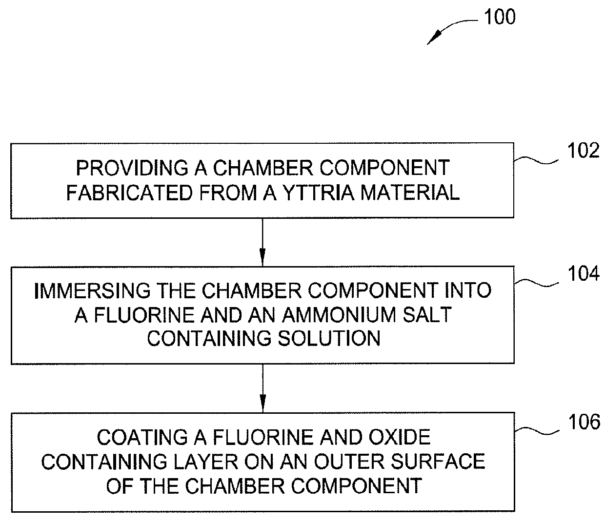
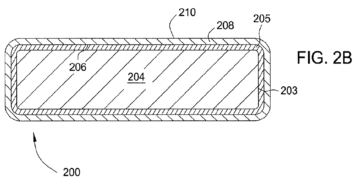
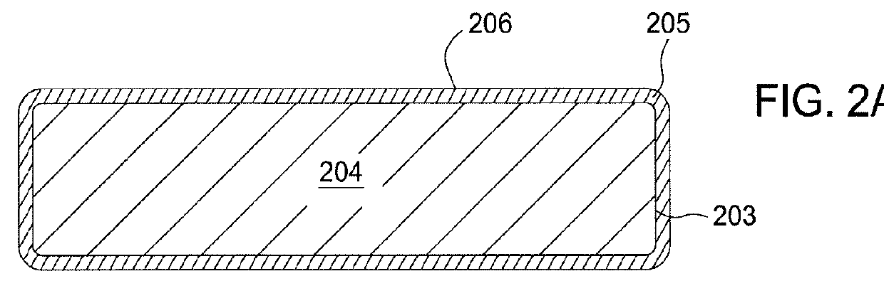
[0016]According to one embodiment of the disclosure, a chamber component is provided that includes a body comprising yttria (Y2O3) having a coating layer comprising a fluorine-rich surface formed thereon for use in plasma processing equipment. In one example, the coating layer may be formed using a wet coating process that includes fluorine ion containing solution. Examples of solutions that may be utilized to form the coating layer may include a fluorine containing chemical and ammonium salt that substantially maintain the wet coating solution at a desired pH level and stable ion concentration during the coating process.

[0017]In one embodiment, the coating layer formed on the chamber component may have a thickness between about 10 nm and about 80 nm. The coating layer maybe amorphous in nature. Surface morphology, corrosion resistance and crystal structure of the coating layer may be formed by bathing the chamber component in a solution comprising fluorine containing chemical and a...


PUM

PropertyMeasurementUnit
thicknessaaaaaaaaaa
thicknessaaaaaaaaaa
densityaaaaaaaaaa

Abstract

Embodiments of the disclosure provide a chamber component for use in a plasma processing chamber apparatus. The chamber component may include a coating layer that provides a fluorine-rich surface. In one embodiment, a chamber component, for use in a plasma processing apparatus, includes a body having an outer layer comprising yttria having a coating layer formed thereon, wherein the coating layer comprises a yttrium fluoride containing material.

Description

CROSS-REFERENCE TO RELATED APPLICATION[0001]This application claims benefit of U.S. Provisional Application Ser. No. 62 / 407,792 filed Oct. 13, 2016 (Attorney Docket No. APPM / 24495L), which is incorporated by reference in its entirety.FIELD[0002]Embodiments disclosed herein generally relate to manufacturing a coating / barrier / passivation layer on a processing chamber component resistive to the corrosive plasma environment utilized in a semiconductor plasma processing chamber. More specifically, embodiments disclosed herein relate to form a fluorine containing layer on a yttria containing structure utilized in plasma equipment components for reduction of particles and stabilization of etch rates and plasma processing conditions in a semiconductor plasma processing chamber.DESCRIPTION OF THE PRIOR ART[0003]Semiconductor processing involves a number of different chemical and physical processes whereby minute integrated circuits are created on a substrate. Layers of materials which make u...

Claims


Application Information

Patent Timeline
19 Apr 2018
Publication
US20180105701A1
IPC
C09D5/08; B05D1/18; C09D1/00; H01L21/67; H01J37/32
CPC
C09D5/08; B05D1/18; C09D1/00; H01L21/67069; H01J37/32495; H01J2237/334; H01J37/32467; H01J37/32477
Inventors
LARSSON, MATS; PAREEK, YOGITA