Surface acoustic wave device with KNb03 piezoelectric thin film, frequency filter, oscillator, electronic circuit, and electronic apparatus

a surface acoustic wave and piezoelectric thin film technology, which is applied in the direction of device material selection, niobium compounds, generators/motors, etc., can solve the problems of large knbo.sub.3 single crystals in the surface acoustic wave device, difficult to produce high quality, and not practical from the perspective of mass production

Inactive Publication Date: 2004-04-13
SEIKO EPSON CORP
View PDF7 Cites 108 Cited by
  • Summary
  • Abstract
  • Description
  • Claims
  • Application Information

AI Technical Summary

Benefits of technology

As a result of the above design, the first oxide thin film layer and the second oxide thin film layer can be made to undergo epitaxial growth in sequence on top of the silicon substrate. A high quality KNbO.sub.3 epitaxial thin film can then be formed on top of the aforementioned layers. Specifically, it becomes an easy matter to form a (010) KNbO.sub.3 epitaxial thin film, making it possible to provide a surface acoustic wave device having a high k.sup.2 which is advantageous with respect to cost and capacity for mass production.
As a result of this design, the k.sup.2 of the piezoelectric thin film forming the surface acoustic wave device that is proved in the electronic circuit's oscillator is high, and integration with an IC is possible. Thus, a small-sized, high-functioning electronic circuit can be provided. The sixth aspect of the present invention is an electronic device characterized in including at least one of the above-described frequency filter, oscillator, and electronic circuit. The k.sup.2 of the piezoelectric thin film in the electronic device is high in this design. As a result, it is possible to offer a small-sized, high-functioning electronic device.

Problems solved by technology

However, conventional surface acoustic wave devices have the following problems.
Namely, it is difficult to produce high quality, large KNbO.sub.3 single crystals in a surface acoustic wave device that uses a KNbO.sub.3 single crystal.
As a result, this is not practical from the perspective of mass production.
However, even if the orientation of the KNbO.sub.3 thin film can be controlled using a SrTiO.sub.3 substrate, it is difficult to form a SrTiO.sub.3 substrate which is larger than two inches.
Accordingly, this also is not suitable from the perspective of mass production.
Furthermore, even if such a substrate could be produced hypothetically, it is not viewed to be practical in terms of cost.
Still, it is difficult to obtain a high-quality epitaxial thin film even when the KNbO.sub.3 thin film is formed directly on top of the Si substrate, because of lattice mismatches and the like.
As a result, a high k.sup.2 cannot be obtained.
However, when providing an electrode on top of the piezoelectric thin film, there is some concern that the piezoelectric thin film may be degraded by water or the like during the electrode forming process.
As a result, formation of the frequency filter becomes troublesome and costs rise.

Method used


Image

  • Surface acoustic wave device with KNb03 piezoelectric thin film, frequency filter, oscillator, electronic circuit, and electronic apparatus
  • Surface acoustic wave device with KNb03 piezoelectric thin film, frequency filter, oscillator, electronic circuit, and electronic apparatus
  • Surface acoustic wave device with KNb03 piezoelectric thin film, frequency filter, oscillator, electronic circuit, and electronic apparatus

Examples


embodiment 1

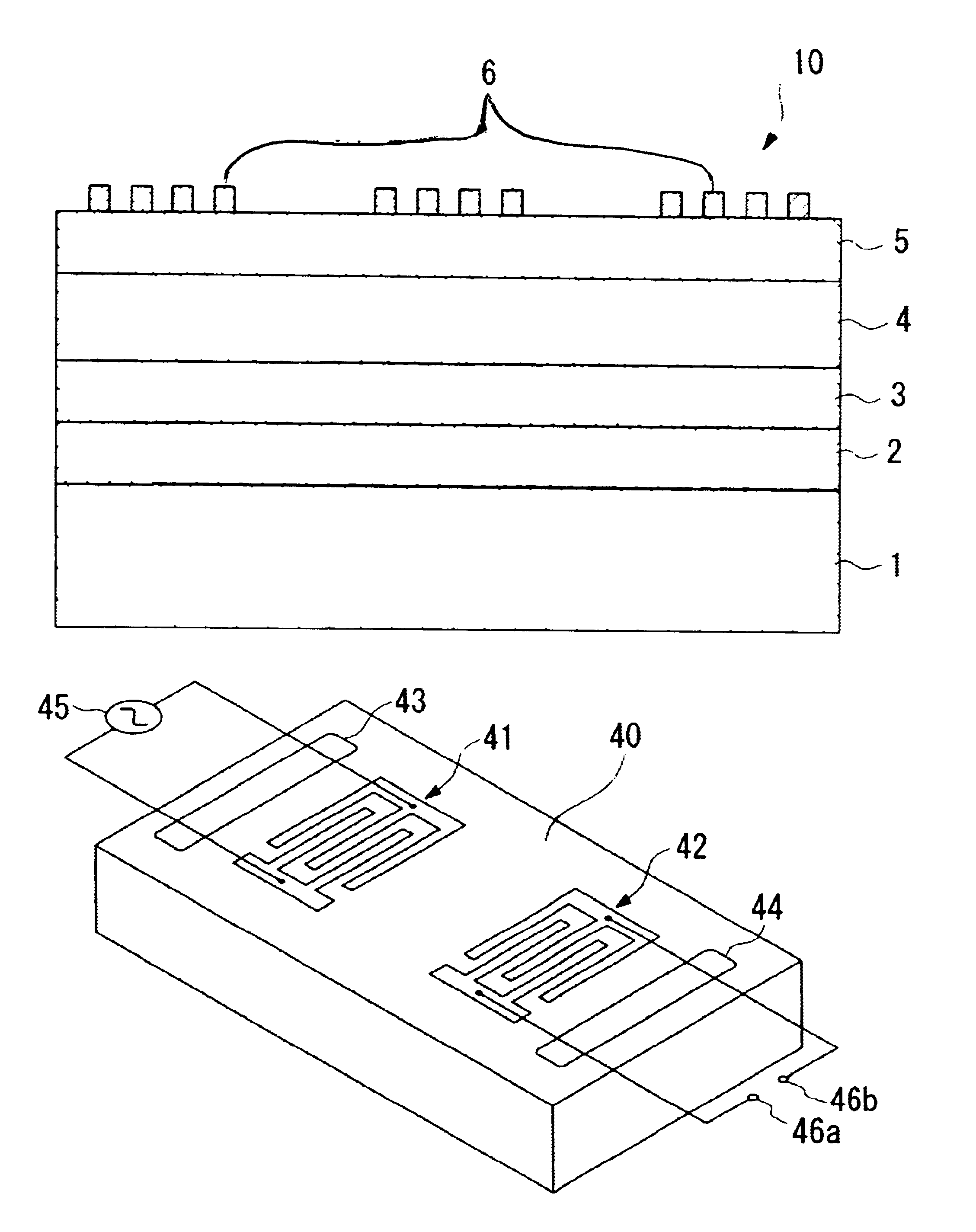
FIG. 1 is a view showing the cross-sectional structure of the surface acoustic wave device according to the first embodiment of the present invention. This surface acoustic wave device is formed of a Si substrate 1, a first oxide thin film layer 2, a second oxide thin film layer 3, a potassium niobate thin film (KNbO.sub.3 thin film) 4, a thin film 5 comprising an oxide or nitride as a protective layer, and electrodes 6. When viewed from above, these electrodes 6 are shaped like IDT electrodes 41, 42, 51, 52, 53 as shown in FIGS. 3 and 4, for example.

The process for forming the surface acoustic wave device of this embodiment consisting of the above-described structure will now be specifically shown. First, a strontium oxide (denoted as "SrO" hereinafter) thin film is formed using a laser ablation method on top of Si (110) single crystal substrate 1 to serve as first oxide thin film layer 2. Film formation was carried out at a substrate temperature of 700.degree. C. in oxygenated pla...

embodiment 2

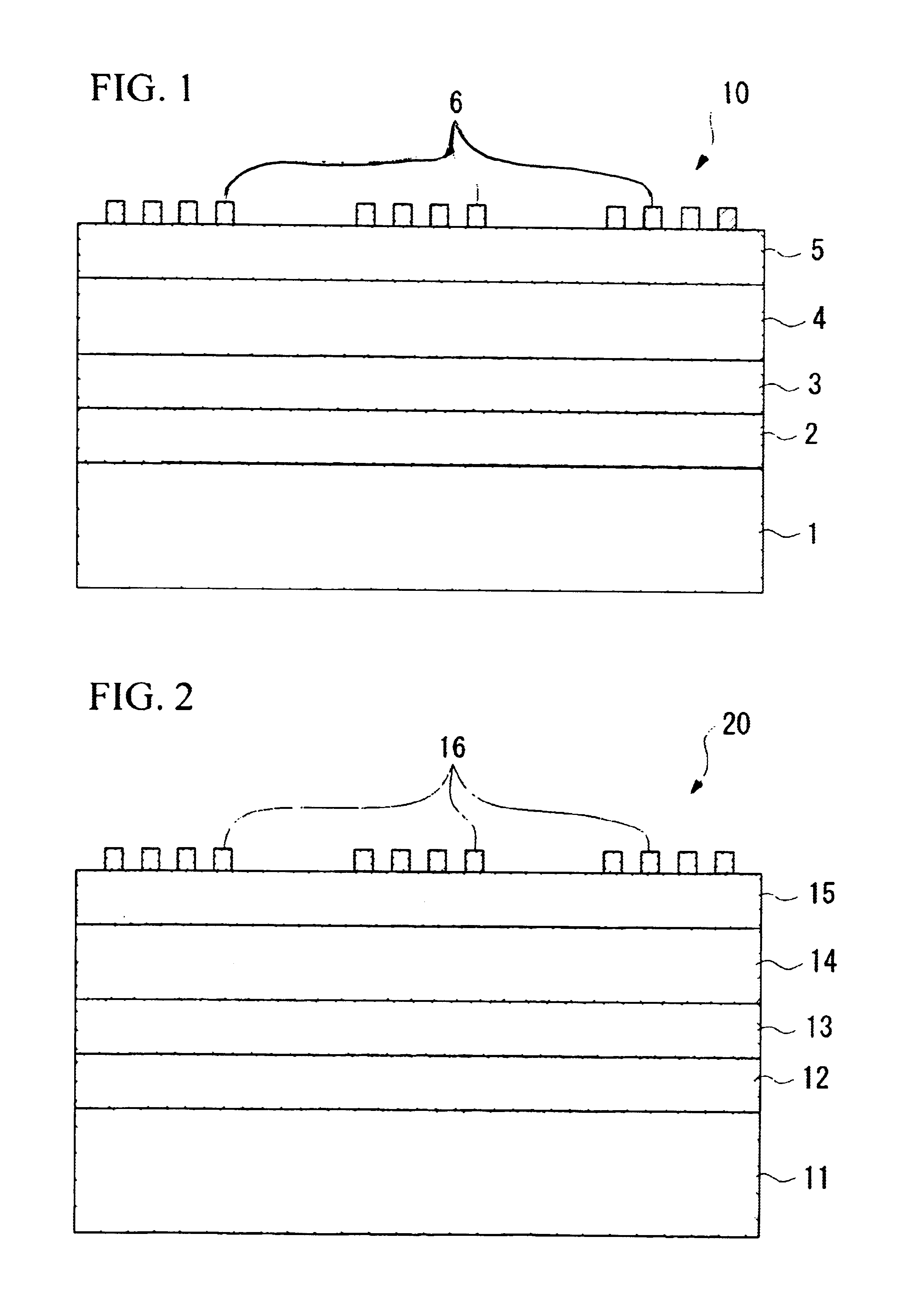
FIG. 2 is a view showing the cross-sectional structure of the surface acoustic wave device according to the second embodiment of the present invention. This surface acoustic wave device is formed of a Si substrate 11, a first oxide thin film layer 12, a second oxide thin film layer 13, KNbO.sub.3 thin film 14, a thin film 15 comprising an oxide or nitride as a protective layer, and electrodes 16. When viewed from above, electrodes 16 are shaped like IDT electrodes 41, 42, 51, 52, and 53 as shown in FIGS. 3 and 4, for example.

The process for forming a surface acoustic wave device according to this embodiment consisting of the above-described structure will be specifically shown. First, a celium oxide (denoted as "CeO.sub.2 " hereinafter) thin film is formed using a laser ablation method on top of a Si (100) single crystal substrate 11 as the first oxide thin film layer 12. Film formation was performed at a substrate temperature of 500.degree. C. in oxygenated plasma at 1.3.times.10.s...

embodiment 3

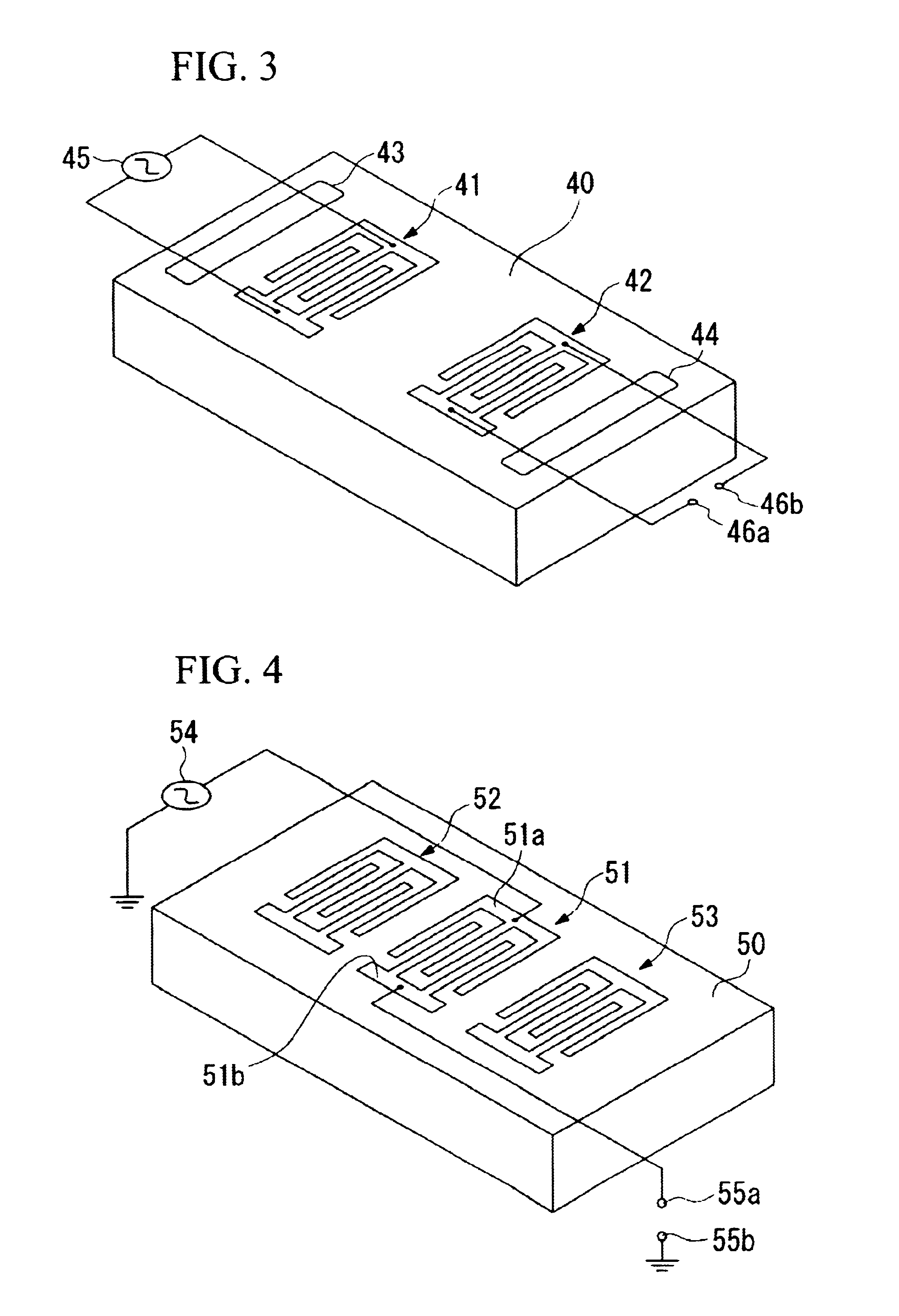
FIG. 3 is a perspective view showing the outer appearance of the frequency filter according to the present embodiment. The frequency filter shown in FIG. 3 has a substrate 40. This substrate 40 is formed by sequentially stacking onto the (110) Si substrate 1 shown in FIG. 1, for example, a first oxide (SrO or MgO) layer 2, a second oxide layer (SrTiO.sub.3) 3, a KNbO.sub.3 piezoelectric thin film 4, and a protective layer (SiO.sub.2 layer or AlN layer) 5, or by sequentially stacking onto the (100) Si substrate 11 shown in FIG. 2, a first oxide (CeO.sub.2, ZrO.sub.2 or YSZ) layer 12, a second oxide layer (SrTiO.sub.3 layer) 13, a KNbO.sub.3 piezoelectric thin film 14, and a protective layer (SiO.sub.2 layer or AlN layer) 15.

IDT electrodes (i.e., Interdigital Transducers) 41 and 42 are formed to the upper surface of substrate 40. IDT electrodes 41 and 42 are formed of Al or an Al alloy, for example, and are designed to have a thickness that is 1 / 100.sup.th of the pitch of the electrod...


PUM

PropertyMeasurementUnit
thicknessaaaaaaaaaa
speedaaaaaaaaaa
frequencyaaaaaaaaaa

Abstract

Surface acoustic wave device having a high k<2>, and a frequency filter, oscillator, electronic circuit and electronic device employing this surface acoustic wave device is provided, wherein a first oxide thin film layer comprising SrO or MgO and a second oxide thin film layer comprising SrTiO3 are sequentially formed on top of a (110) Si substrate, or a first oxide thin film layer comprising CeO2, ZrO2 or yttrium-stabilized zirconia and a second oxide thin film layer comprising SrTiO3 are sequentially formed on top of a (100) Si substrate, a KNbO3 piezoelectric thin film being then formed on top of either of these second oxide thin film layers, and then, a protective film comprising oxide or nitride is formed on top of the KNbO3 piezoelectric thin film, finally, at least one electrode is formed on top of this protective film, to form a surface acoustic wave device, which surface acoustic wave device is employed to form a frequency filter, oscillator, electronic circuit, or electronic device.

Description

1. Field of the InventionThe present invention relates to a surface acoustic wave device having a piezoelectric thin film, a frequency filter, a oscillator, an electronic circuit and an electronic apparatus, and more specifically, to a surface acoustic wave device having a silicon substrate and a potassium niobate piezoelectric thin film, a frequency filter, a oscillator, an electronic circuit, and an electronic apparatus, which are employed in the telecommunications field.2. Description of the Related ArtSurface acoustic wave devices employing a piezoelectric material with a high electromechanical coupling coefficient (denoted as "k.sup.2 " hereinafter) have been desired in order to improve the performance of non-lead containing surface acoustic wave devices. Lithium niobate is known conventionally as a material with a high k.sup.2, demonstrating a k.sup.2 of 5.5% using Rayleigh waves. However, it has been shown that k.sup.2 can exceed 50% with potassium niobate ("KNbO.sub.3 " here...

Claims


Application Information

Patent Timeline
Patent Type & Authority Patents(United States)
IPC IPC(8): H03H9/02C30B29/30H01L41/08H01L41/09C01G33/00H01L41/18H03B5/30H03H9/05H03H9/145H03H9/25H03H9/72
CPCH03H9/02574H03H9/02984H03H9/0542
Inventor IWASHITA, SETSUYAHIGUCHI, TAKAMITSUMIYAZAWA, HIROMU
Owner SEIKO EPSON CORP
Why Eureka
Try Eureka