Semiconductor device for directly converting radioisotope emissions into electrical power

a technology of radioisotopes and semiconductor devices, which is applied in semiconductor devices, radiation electrical energy, nuclear engineering, etc., can solve the problems of difficult to efficiently convert tritium beta emissions into usable electrical power, radiation energy may also be harmful to operators in the vicinity of batteries, and low energy of tritium beta emissions

Active Publication Date: 2018-04-19
CITY LABS
View PDF5 Cites 8 Cited by
  • Summary
  • Abstract
  • Description
  • Claims
  • Application Information

AI Technical Summary

Problems solved by technology

However, in the hopes of achieving reasonable power levels, the radioisotope of choice often emitted unsafe amounts of high energy radiation that would either quickly degrade semiconductor device properties within the betavoltaic battery or the surrounding electronic devices powered by the battery.
The radiated energy may also be harmful to operators in the vicinity of the battery.
Unfortunately, tritium's beta emissions are so low in energy that it is has been difficult to efficiently convert these emissions into usable electrical power for even the lowest power applications, such as powering an SRAM memory to prevent loss of stored data.
However, this approach is extremely inefficient with respect to the beta energy emissions entering the semiconductor (less than about 1%).
In short, the polycrystalline and amorphous semiconductors have a high number of defects resulting in recombination centers for the EHPs, which in turn significantly reduce the betavoltaic current and lead to very low efficiency for the battery.
However, their low efficiency makes them a poor choice for even the lowest power applications, such as for use in SRAM memory devices.
However, AlGaAs homojunctions cells are difficult to reproduce consistently with uniform dark currents across a semiconductor device due to the oxidation of the aluminum.
As a result, AlGaAs is also an expensive option to scale up.
Safety concerns over containment of the tritium based betavoltaic battery have emerged as another obstacle to commercialization of a tritium battery.
Many accidents involving tritium release due to the breakage of the tritium vials in EXIT signs have caused public concerns and resulted in costly clean-up operations.
However, the solid-state tritium metal hydride still involves a miniscule amount of tritium release when open to the environment at room temperature.
Although several tritium based batteries have been proposed including direct conversion devices built within an integrated circuit, a method of effectively hermetically packaging the battery containing the tritium metal hydride continues to be problematic.
A major obstacle to hermetically sealing this type of battery is the risk associated with using a sealing process that involves high temperatures, i.e., above 200-300° C. At these temperatures tritium is released from the metal hydride, possibly leading to battery failure after sealing, or worse, causing tritium exposure at the sealing manufacturing facility and to the operator of the sealing equipment.
The problem with such an approach arises when a relatively low energy radioisotope such as tritium is used.
Unfortunately, alterations to the semiconductor surface risk increasing lattice defects, resulting in a high number of recombination centers for EHPs.
This creates a direct conversion semiconductor device with a low open circuit voltage and reduced short circuit current, with a resulting low overall efficiency.

Method used


Image

  • Semiconductor device for directly converting radioisotope emissions into electrical power
  • Semiconductor device for directly converting radioisotope emissions into electrical power
  • Semiconductor device for directly converting radioisotope emissions into electrical power

Examples


Embodiment Construction

[0049]Before describing in detail the particular methods and apparatuses related to tritium direct conversion semiconductor devices, it should be observed that the present invention resides primarily in a novel and non-obvious combination of elements and process steps. So as not to obscure the disclosure with details that will be readily apparent to those skilled in the art, certain conventional elements and steps have been presented with lesser detail, while the drawings and the specification describe in greater detail other elements and steps pertinent to understanding the invention.

[0050]The following embodiments are not intended to define limits as to the structure or method of the invention, but only to provide exemplary constructions. The embodiments are permissive rather than mandatory and illustrative rather than exhaustive.

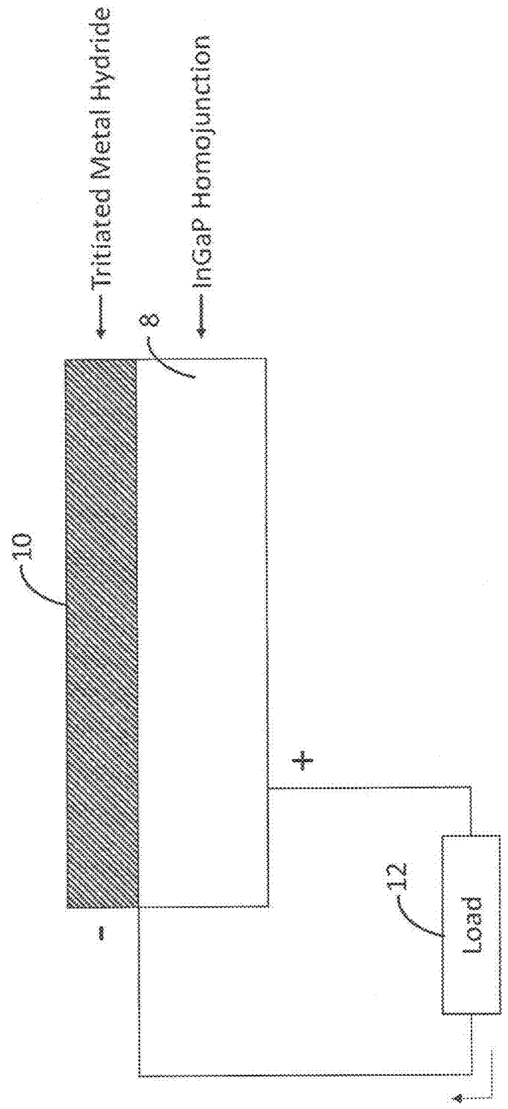
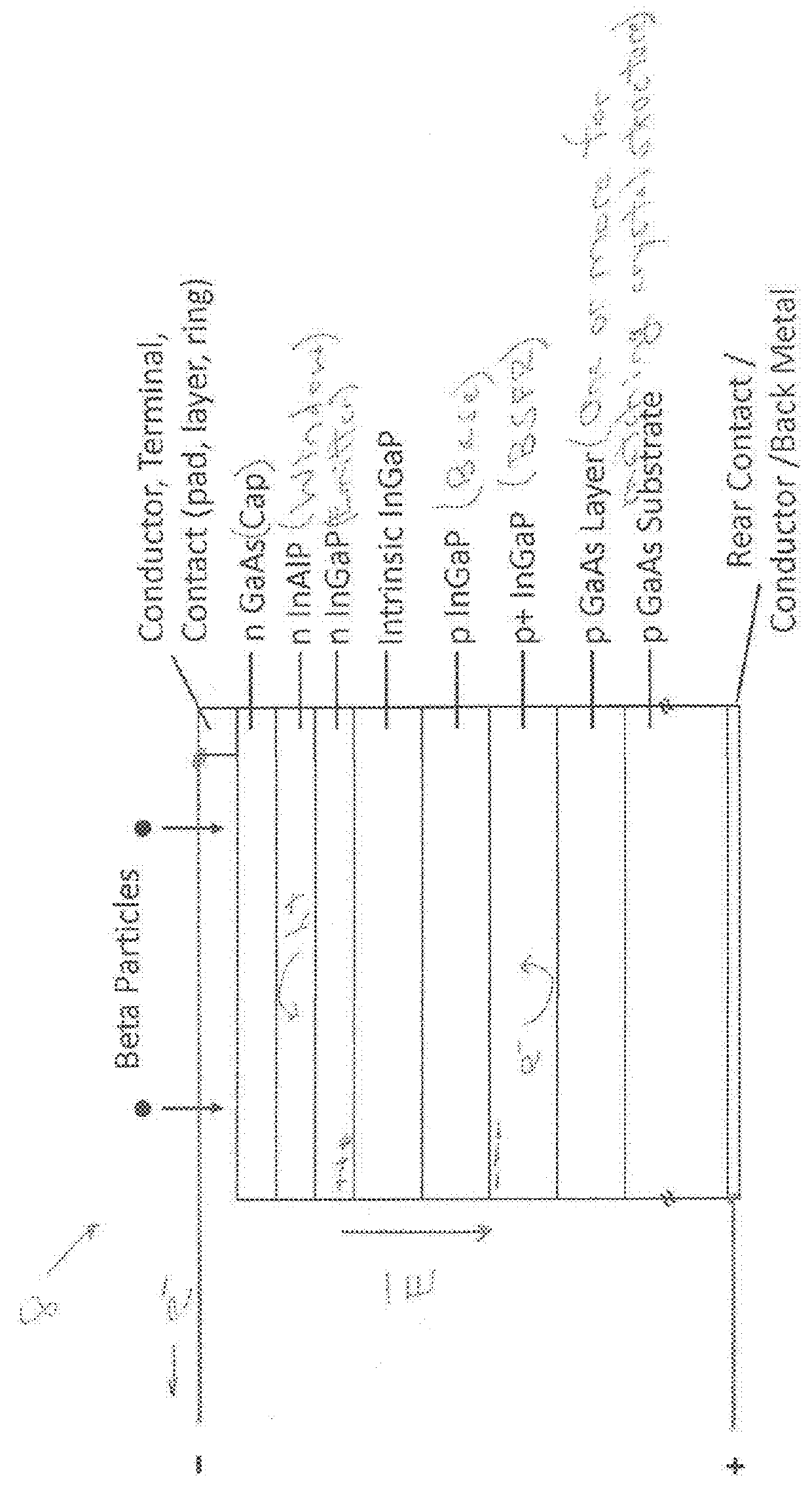
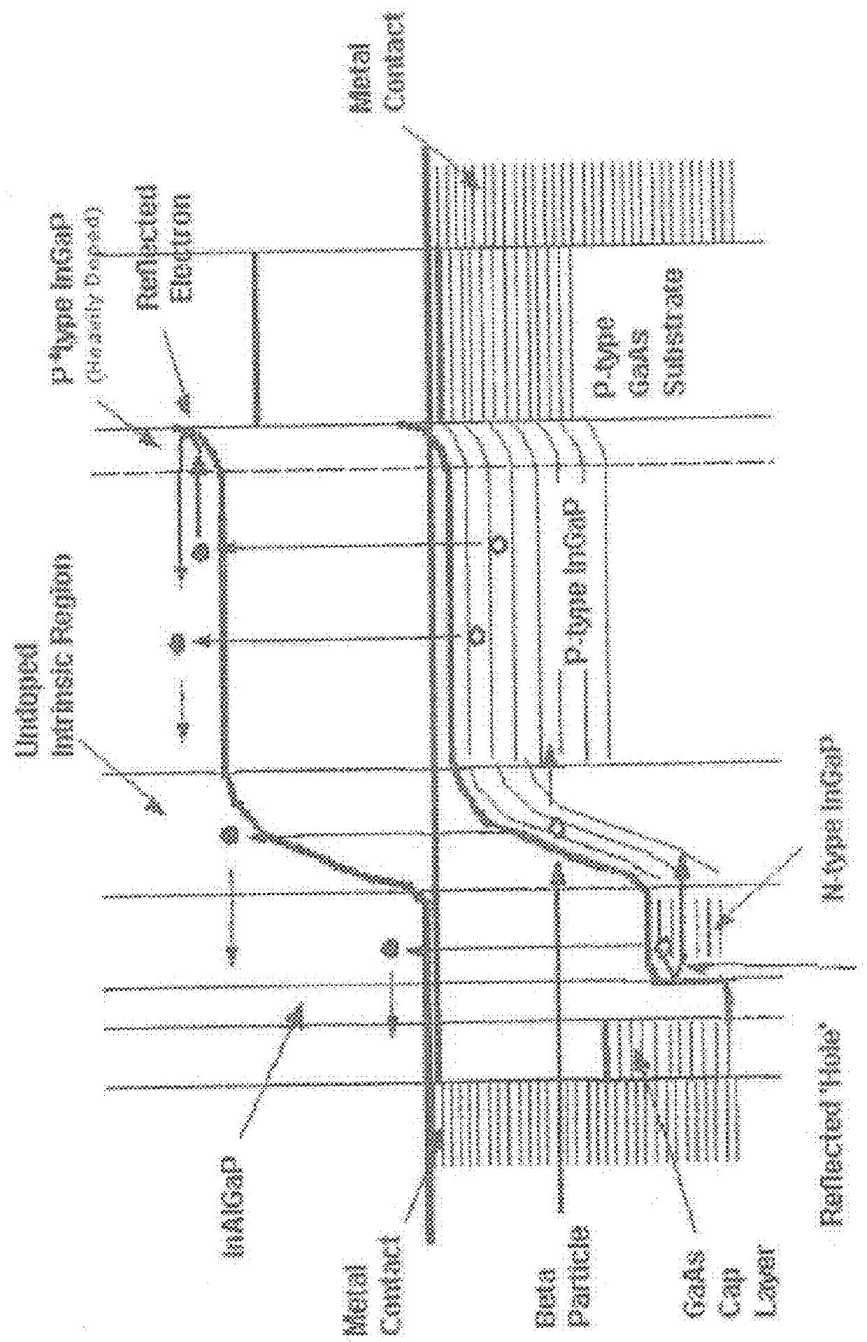
[0051]The present invention is described in the context of a tritium direct conversion semiconductor device comprising a single crystal semiconductor. In...


PUM


Abstract

A device for producing electricity. In one embodiment, the device comprises a doped germanium or a doped GaAs substrate and a plurality of stacked material layers (some of which are doped) above the substrate. These stacked material layers, which capture the beta particles and generate electrical current, may include, in various embodiments, GaAs, InAlP, InGaP, InAlGaP, AlGaAs, and other semiconductor materials. A beta particle source generates beta particles that impinge the stack, create electron-hole pairs, and thereby generate electrical current. In another embodiment the device comprises a plurality of epi-liftoff layers and a backing support material.

Description

CROSS REFERENCE TO RELATED APPLICATIONS[0001]The present application is a continuation-in-part application of parent application Ser. No. 14 / 623,861, filed on Feb. 17, 2015 (Attorney Docket Number 11432-008), now U.S. Pat. No. 9,799,419, which claims priority under 35 U.S.C. 119(e) to the provisional patent application filed on Feb. 17, 2014 and assigned application No. 61 / 940,571. The parent and provisional patent applications are both incorporated in their entirety herein.BACKGROUND OF THE INVENTION[0002]The direct conversion of radioisotope beta (electron) emissions into usable electrical power via beta emissions directly impinging on a semiconductor junction device was first proposed in the 1950's. Incident beta particles absorbed in a semiconductor create electron-hole-pairs (EHPs) which are accelerated by the built-in field to device terminals, and result in a current supplied to a load. These devices are known as direct conversion semiconductor devices, beta cells, betavoltai...

Claims


Application Information

Patent Timeline
Patent Type & Authority Applications(United States)
IPC IPC(8): G21H1/06H01L31/0232H01L31/0304H01L31/0216H01L31/115H01L31/18
CPCG21H1/06H01L31/02327H01L31/03046H01L31/0304H01L31/02161H01L31/115H01L31/1844H01L31/184H01L31/1892
Inventor CABAUY, PETER
Owner CITY LABS
Why Eureka
Try Eureka