
Semiconductor device, display device, and electronic device

a technology of display device and semiconductor device, which is applied in the direction of pulse generator, pulse technique, instruments, etc., can solve the problems of increasing the number of transistors included in the level shifter, and the number of voltages for operating the level shifter, so as to reduce the number of transistors in reduce the number of voltages for operating the circuit serving as the level shifter

Active Publication Date: 2018-05-31
SEMICON ENERGY LAB CO LTD
View PDF16 Cites 20 Cited by
  • Summary
  • Abstract
  • Description
  • Claims
  • Application Information

AI Technical Summary

Benefits of technology

The present invention provides a semiconductor device that can serve as a level shifter and a display device, electronic device, and the like. The semiconductor device has a novel structure that can be formed over a panel as well as a transistor in a display portion and includes a controller IC (including a frame memory, a timing controller, and the like) necessary for refreshing an image. The semiconductor device also has a reduced number of transistors in a circuit serving as a level shifter, a reduced number of voltages for operating a circuit serving as a level shifter, and a reduced number of pixels needed for the display. These features can help to further reduce the power consumption and improve the overall performance of the semiconductor device and the display device, electronic device, and the like.

Problems solved by technology

However, an increase in the number of transistors included in the level shifter and the number of voltages for operating the level shifter is a problem.

Method used


Image

  • Semiconductor device, display device, and electronic device
  • Semiconductor device, display device, and electronic device
  • Semiconductor device, display device, and electronic device

Examples


embodiment 1

[0091]In this embodiment, a semiconductor device of one embodiment of the present invention will be described. The semiconductor device has a function of boosting the amplitude voltage of an input signal and outputting the resulting signal as an output signal. Thus, the semiconductor device is referred to as a boosting circuit or a level shifter in some cases. Note that a device including an element that can utilize semiconductor characteristics, such as a circuit including a transistor or a capacitor, is a semiconductor device.

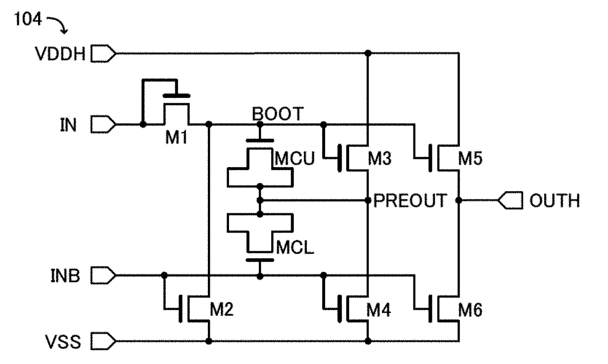
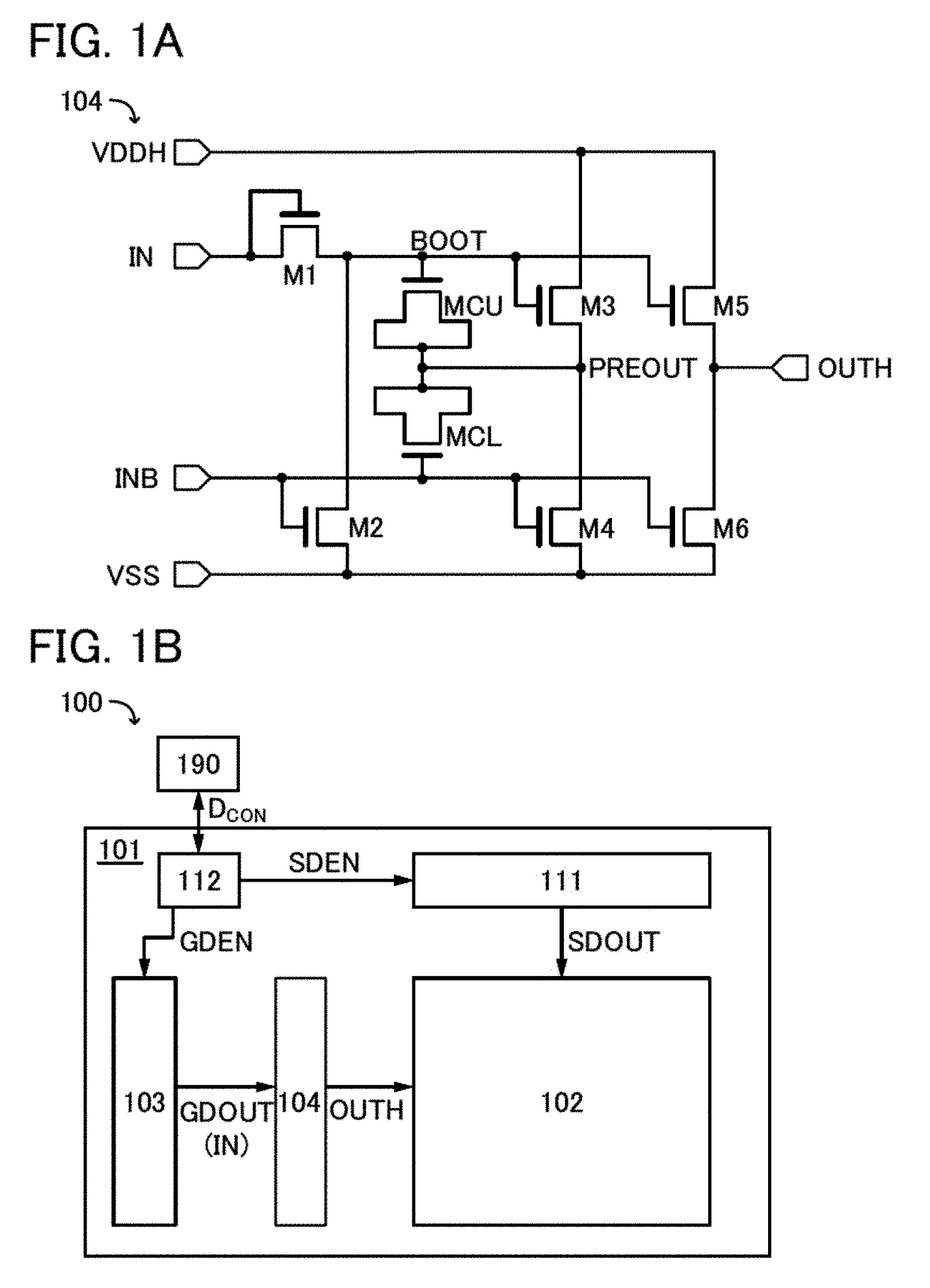
[0092]FIG. 1A is a circuit diagram of a level shifter 104 that is a semiconductor device of one embodiment of the present invention.

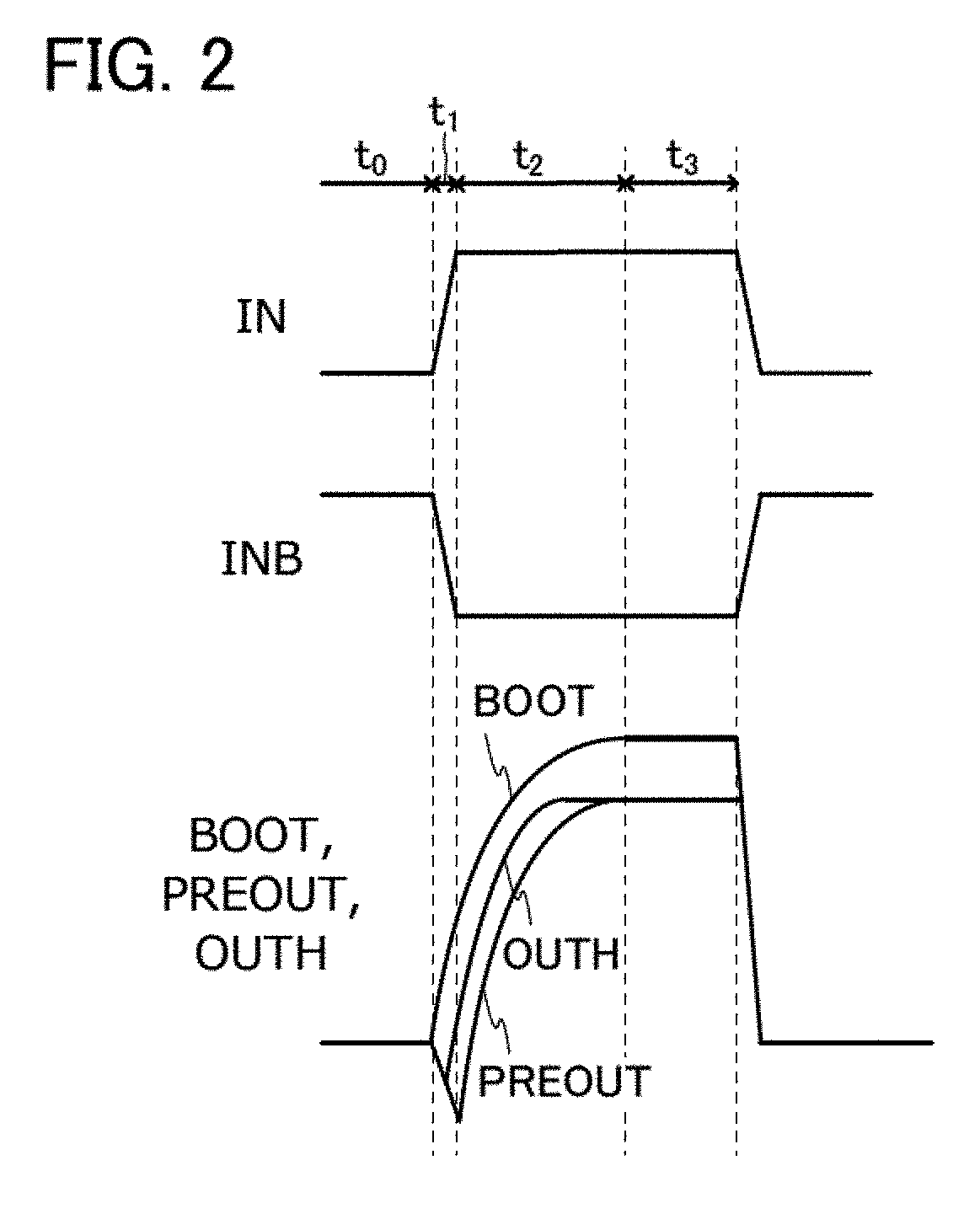
[0093]The level shifter 104 includes transistors M1 to M6, a capacitor MCU, and a capacitor MCL. FIG. 1A illustrates an input signal IN, an inverted input signal INB, an output signal OUTH, a voltage VDDH, a voltage VSS, a node BOOT, and a node PREOUT.

[0094]A wiring to which the input signal IN is supplied is connected to a gate ...

embodiment 2

[0159]In this embodiment, an appearance of the display device 100 described in Embodiment 1 and a structure example that can be applied to the base 101 will be described.

[0160]FIG. 18A illustrates an example of an appearance of the display device described in aforementioned Embodiment 1 on which the level shifter can be mounted. The display device 100 is a display device including one of a liquid crystal element, a light-emitting element, and the like as a display element, and the display element is included in a display portion 102.

[0161]The display device 100 includes the display portion 102, a gate driver 103, a level shifter 104, a source driver IC 111, and a controller IC 112 over the base 101. The display portion 102, the gate driver 103, and the level shifter 104 are formed over the base 101. The source driver IC 111 and the controller IC 112 are mounted as components of an IC chip or the like, over the base 101 with use of an anisotropic conductive adhesive or an anisotropic...

embodiment 3

[0190]In this embodiment, a circuit other than a level shifter that can be formed over the base 101 applicable to the display device 100 described in Embodiment 2 will be described.

[0191]A pixel circuit included in the display portion 102 and a pixel circuit included in the display portion 106 are described.

[0192]The pixel circuit in the display portion 102 includes one kind of a display element such as a liquid crystal element or a light-emitting element. The configuration of the pixel circuit in the display portion 102 depends on the kind of display element.

[0193]FIG. 21A illustrates an example of a pixel circuit in which a liquid crystal element is used as a display element of the display portion 102. A pixel circuit 21 includes a transistor Tr1, a capacitor C1, and a liquid crystal element LD.

[0194]A first terminal of the transistor Tr1 is electrically connected to a wiring SL, a second terminal of the transistor Tr1 is electrically connected to a first terminal of the liquid cr...


PUM


Abstract

A level shifter including a transistor that can be formed through the same process as a display portion is provided. A semiconductor device serves as a level shifter including transistors having the same conductivity type. The semiconductor device includes a so-called MIS capacitor in which metal, an insulator, and a semiconductor are stacked as a capacitor for boosting an input signal. Since the MIS capacitor is used, the gate-source voltage of a transistor for generating an output signal can be increased. Thus, boosting operation to generate the output signal can be performed more surely.

Description

BACKGROUND OF THE INVENTION1. Field of the Invention[0001]Embodiments of the present invention relate to a semiconductor device, a display device, and an electronic device.2. Description of the Related Art[0002]Display devices included in mobile phones such as smartphones, tablet information terminals, and notebook personal computers (PC) have undergone various improvements in recent years. For example, there have been developed display devices with features such as higher resolution, higher color reproducibility (higher NTSC ratio), a smaller driver circuit, and lower power consumption.[0003]As an example, an improved display device has a function of automatically adjusting the brightness of an image displayed on the display device in accordance with ambient light. An example of such a display device is a display device having a function of displaying an image by reflecting ambient light and a function of displaying an image by making a light-emitting element emit light. This struc...

Claims


Application Information

Patent Timeline
Patent Type & Authority Applications(United States)
IPC IPC(8): H01L27/12H03K3/356G09G3/36
CPCH01L27/124H03K3/356017H01L27/1225G09G3/3648G09G2310/0289G06F3/0412G09G3/3233G09G3/3266G09G3/3677G09G2300/046H01L27/1255G09G3/20G09G2330/021G09G2300/0426G11C19/28G11C19/14
Inventor INOUE, HIROKIAKASAWA, FUMIKA
Owner SEMICON ENERGY LAB CO LTD
Learn More