Method for the production of wafers of nitride of element 13, having a non-zero truncation angle

a technology of nitride and element 13, which is applied in the direction of basic electric elements, electrical equipment, crystal growth process, etc., can solve the problems of limiting the performance and the lifespan of group-13-element nitride-based components, certain unfavorable properties of element nitride layers, and achieve the effect of facilitating the separation of the first group-13-element nitride layer

Active Publication Date: 2018-06-07
IV WORKS
View PDF6 Cites 0 Cited by
  • Summary
  • Abstract
  • Description
  • Claims
  • Application Information

AI Technical Summary

Benefits of technology

[0065]The annealing step facilitates separation of the first group-13-element nitride layer by convertin

Problems solved by technology

However, the heteroepitaxy technique induces numerous crystal defects in the group-13-element nitride structure, such as dislocations, limiting the performance and the lifespan of group-13-element nitride-based components.
The optoelectronic components produced on zero offcut group-13-element nitride layers have certain unfavorable properties such as high surface roughness of the epitaxial layers, or a lower capacity to incorporate elements such as indium, for example.
However, even if epitaxial growth on

Method used


Image

  • Method for the production of wafers of nitride of element 13, having a non-zero truncation angle
  • Method for the production of wafers of nitride of element 13, having a non-zero truncation angle
  • Method for the production of wafers of nitride of element 13, having a non-zero truncation angle

Examples


Embodiment Construction

[0080]Various exemplary methods of fabricating semiconductor wafers, and of the wafers thus obtained, will now be described in further detail in reference to the figures.

[0081]In these various figures, the equivalent elements bear the same numerical labels. The method according to the invention will be described below in reference to the fabrication of gallium nitride GaN wafers.

[0082]However, it is quite obvious to the person skilled in the art that the method described below may be used to grow a material including a group-13-element nitride layer other than gallium nitride GaN.

1. Fabrication Method

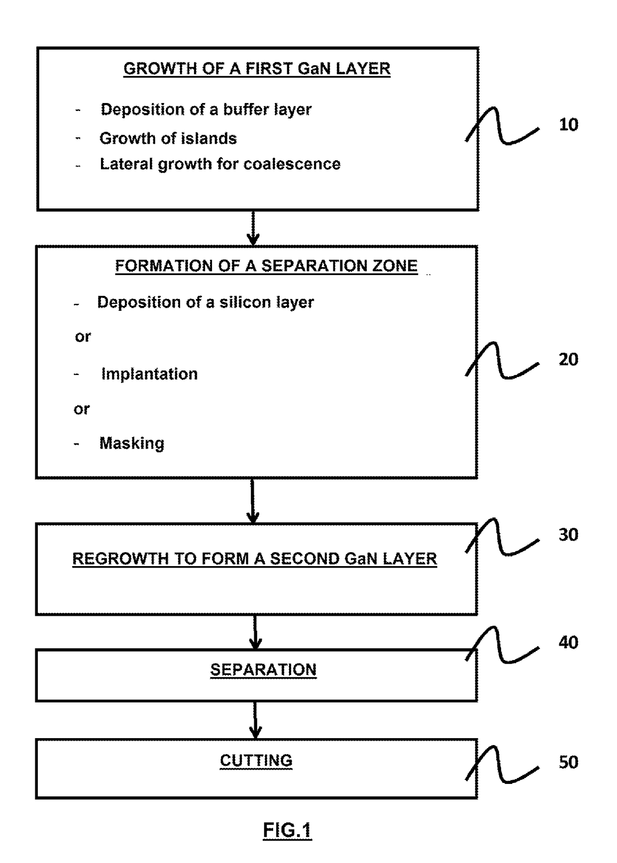
[0083]The main phases of the method of fabricating GaN wafers are illustrated in FIG. 1.

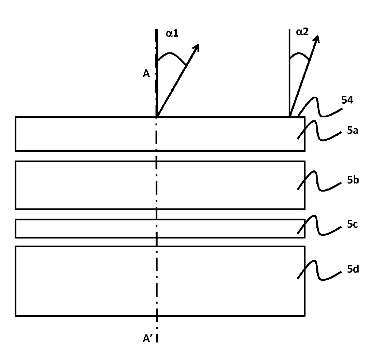
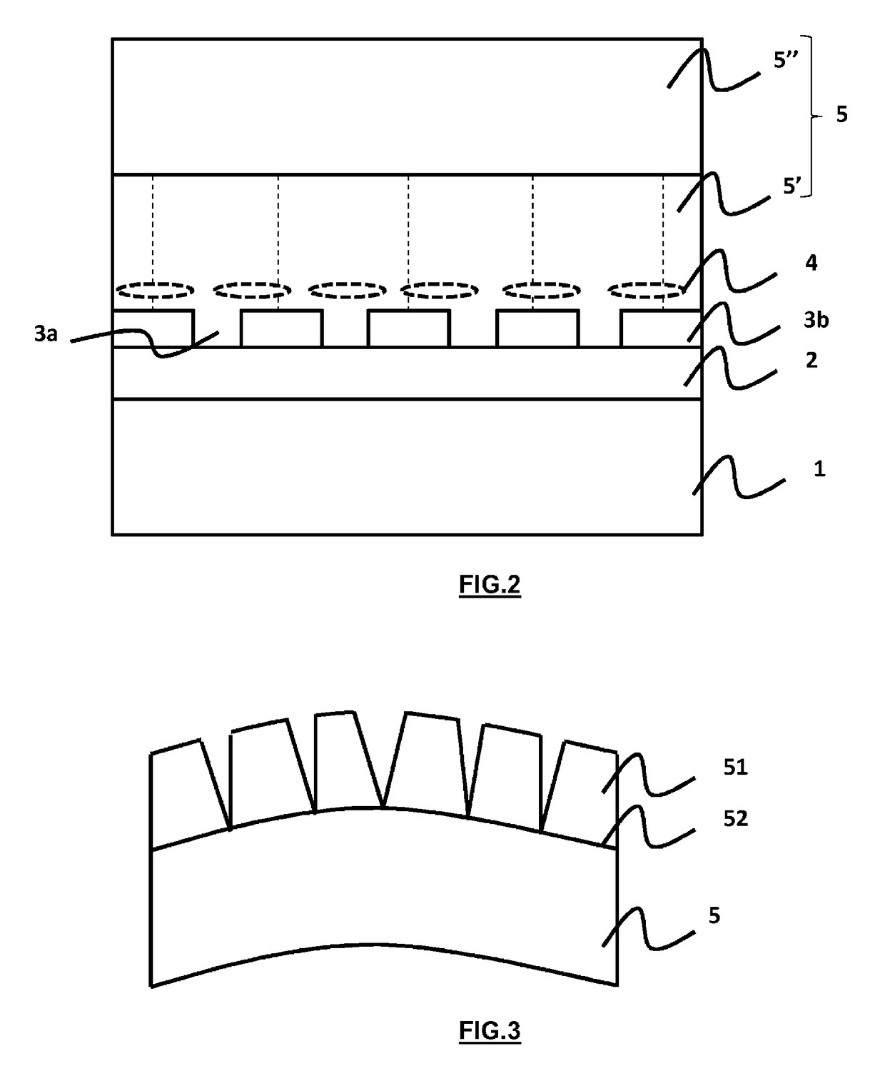
[0084]The method comprises:[0085]i) a growth phase 10 of a first GaN layer 5′,[0086]ii) a formation phase 20 of a separation zone 4,[0087]iii) an epitaxial regrowth phase 30 to form a second thick GaN layer 5″,[0088]iv) a separation phase 40 to obtain a GaN crystal 5,[0089]v) a cutting phase 50 of th...


PUM


Abstract

The invention relates to a method for production of wafers of nitrides of element (13) (5a, 5b, 5c, 5d) from a self-supported crystal of nitride of element (13), extending longitudinally along a main axis orthogonal to a growth face of the crystal and passing through the centre of said growth face, the crystal (10) having a truncation angle with a non-zero value, remarkable in that the method comprises a phase of cutting the self-supported crystal along the transverse cutting planes of the crystal in order to obtain wafers of nitride of element (13), each wafer including a front face having a non-zero truncation angle in the vicinity of the centre of the front face.

Description

[0001]TECHNICAL FIELD[0002]The invention relates to the general technical field of fabricating semiconductor material based on elements of groups 13 and 15 of the periodic table—such as gallium nitride GaN.[0003]Notably, the present invention relates to the fabrication of group-13-element nitride wafers having a non-zero offcut angle.[0004]In the context of the present invention, the offcut angle at a point on the surface of a wafer is defined by the angle between:[0005]the normal to a front face of the group-13-element nitride wafer (normal at the point for which the offcut angle is defined) and[0006]the normal (also known as the c-axis) to a c-oriented (0001) crystal plane (normal to the crystal plane at the aforesaid point).[0007]Such a group-13-element nitride wafer may be intended for the production of semiconductor structures such as light-emitting diodes (LEDs) or laser diodes (LDs).PRESENTATION OF THE PRIOR ART[0008]The current methods of fabricating semiconductor materials ...

Claims


Application Information

Patent Timeline
IPC IPC(8): C30B29/40C30B25/04C30B25/18C30B33/00
CPCC30B29/406C30B25/04C30B25/18C30B33/00H01L33/32C30B29/403H01L21/02002
Inventor BEAUMONT, BERNARDLE ROUX, VIANNEYCOLE, JASON
Owner IV WORKS
Why Eureka
Try Eureka