Atomic Layer Etch Process Using Plasma In Conjunction With A Rapid Thermal Activation Process

Active Publication Date: 2018-06-14
MATTSON TECHNOLOGY +1
View PDF8 Cites 5 Cited by
  • Summary
  • Abstract
  • Description
  • Claims
  • Application Information

AI Technical Summary

Benefits of technology

[0006]In general, the present disclosure is directed to a process and apparatus for carrying out a precision controlled etch on a layer, particularly on a layer contained on a semiconductor wafer. In accordance with the present disclosure, the process includes exposing a layer to a reactive species. The reactive species, for instance, can be generated by a plasma source. With the possible screening grid between the plasma source and the substrate, mostly reactive neutral will reach the substrate surface without ion bombardment. While the layer is exposed to the rea

Problems solved by technology

The above traditional method using ion bombardment activation, however, has not been successful on other layers, particularly layers containing carbon and other low dielectric films.
Furth

Method used


Image

  • Atomic Layer Etch Process Using Plasma In Conjunction With A Rapid Thermal Activation Process
  • Atomic Layer Etch Process Using Plasma In Conjunction With A Rapid Thermal Activation Process
  • Atomic Layer Etch Process Using Plasma In Conjunction With A Rapid Thermal Activation Process

Examples


Example

[0016]Reference now will be made in detail to embodiments, one or more examples of which are illustrated in the drawings. Each example is provided by way of explanation of the embodiments, not limitation of the present disclosure. In fact, it will be apparent to those skilled in the art that various modifications and variations can be made to the embodiments without departing from the scope or spirit of the present disclosure. For instance, features illustrated or described as part of one embodiment can be used with another embodiment to yield a still further embodiment. Thus, it is intended that aspects of the present disclosure cover such modifications and variations.

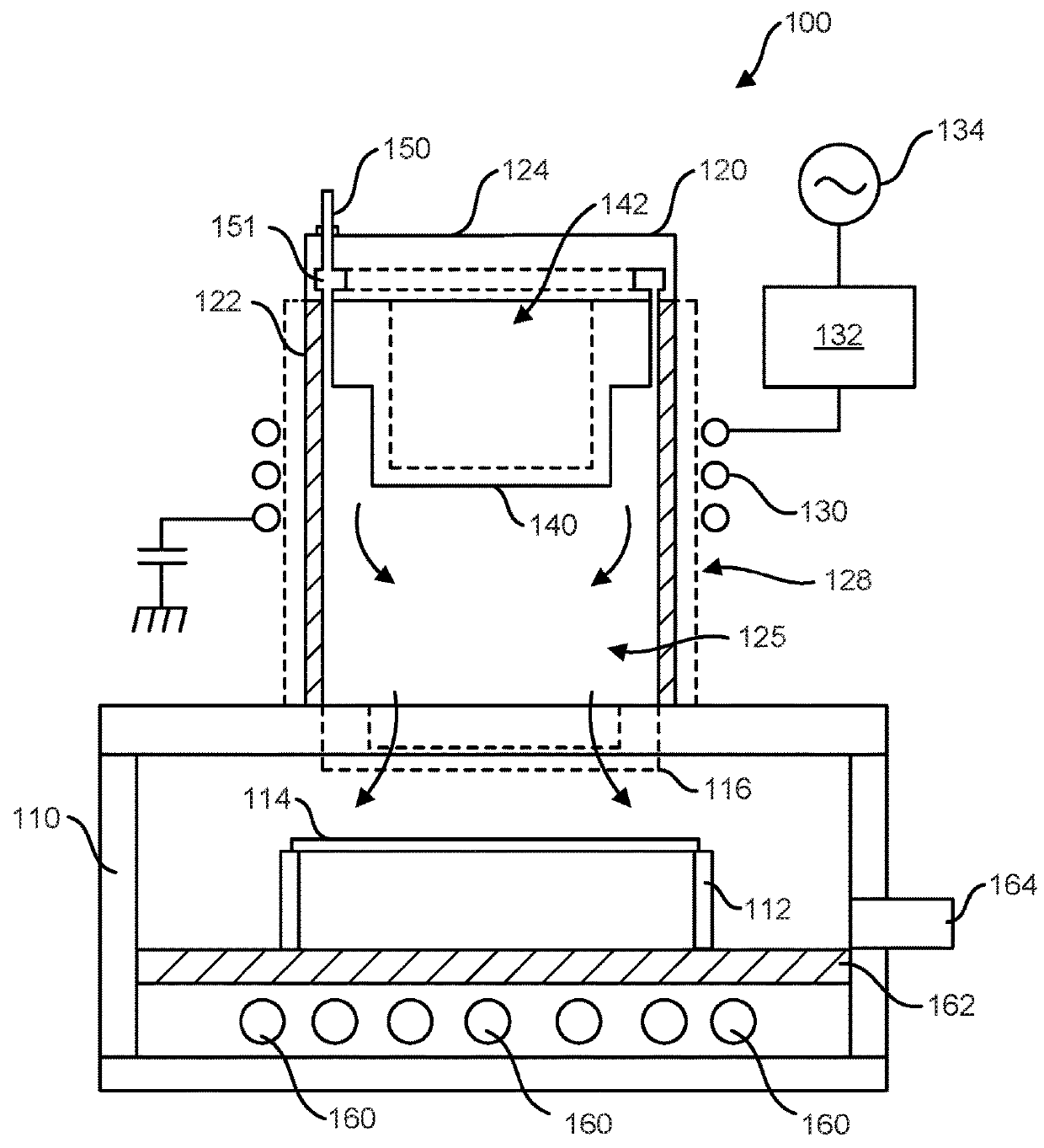
[0017]The present disclosure is generally directed to a process for etching the surface of a substrate, such as a semiconductor wafer. The present disclosure is also directed to an apparatus and system for carrying out the process. In accordance with the present disclosure, the surface of a substrate is contacted with...


PUM


Abstract

A process for etching a film layer on a semiconductor wafer is disclosed. The process is particularly well suited to etching carbon containing layers, such as hardmask layers, photoresist layers, and other low dielectric films. In accordance with the present disclosure, a reactive species generated from a plasma is contacted with a surface of the film layer. Simultaneously, the substrate or semiconductor wafer is subjected to rapid thermal heating cycles that increase the temperature past the activation temperature of the reaction in a controlled manner.

Description

RELATED APPLICATIONS[0001]The present application is based on and claims priority to U.S. Provisional Patent application Ser. No. 62 / 434,036, filed on Dec. 14, 2016, which is incorporated herein by reference,BACKGROUND[0002]Plasma processing is widely used in the semiconductor industry for deposition, etching, resist removal, and related processing of semiconductor wafers and other substrates. Plasma sources (e.g., microwave, ECR, inductive, etc.) are often used for plasma processing to produce high density plasma and reactive species for processing substrates.[0003]One type of process carried out in the past using plasma is atomic layer etching. Atomic layer etching is a technique to perform critical etching with very fine precision for semiconductor device manufacturing. Atomic layer etching is performed on a thin layer while attempting to avoid undue sub-surface damage or undesirable modifications. Atomic layer etching may be performed to etch a very thin layer that overlays anot...

Claims


Application Information

Patent Timeline
IPC IPC(8): H01L21/311H01L21/3105H01J37/32
CPCH01L21/31138H01L21/31058H01J37/32422H01J2237/2001H01J37/32724H01J37/32449H01J2237/3341H01J37/32357H01L21/3065H01L21/324H01L21/027
Inventor MA, SHAWMING
Owner MATTSON TECHNOLOGY
Why Eureka
Try Eureka