Semiconductor package and fabrication method thereof

a technology of semiconductor memory devices and semiconductors, applied in the field of semiconductor memory devices, can solve the problems of limited integration of 2d semiconductor memory devices, high equipment requirements, etc., and achieve the effect of improving defects and improving warpage phenomena

Active Publication Date: 2018-06-14
SAMSUNG ELECTRONICS CO LTD
View PDF2 Cites 25 Cited by
  • Summary
  • Abstract
  • Description
  • Claims
  • Application Information

AI Technical Summary

Benefits of technology

[0005]Example embodiments provide a semiconductor package capable of improving a warpage phenomenon and a process margin and a fabrication method thereof.
[0009]According to the example embodiments, the semiconductor package can improve a warpage phenomenon.
[0010]Further, the semiconductor package can improve defects due to overflow of the adhesive.

Problems solved by technology

For fineness of the patterns, since expensive equipment is required, integration of the 2D semiconductor memory device is limited.

Method used


Image

  • Semiconductor package and fabrication method thereof
  • Semiconductor package and fabrication method thereof
  • Semiconductor package and fabrication method thereof

Examples


Embodiment Construction

[0020]Hereinafter, semiconductor packages and fabrication methods thereof according to example embodiments will be described.

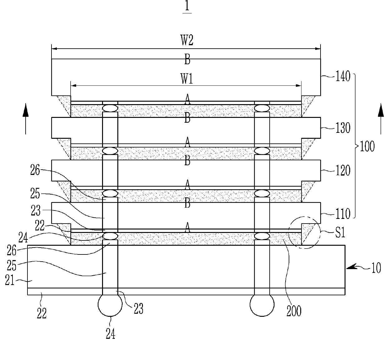
[0021]FIG. 1 is a schematic configuration of a 3D stacked semiconductor package 1 according to an exemplary embodiment.

[0022]Referring to FIG. 1, the 3D stacked semiconductor package 1 (also referred to as the “semiconductor package”) includes a substrate 10 and a 3D stacked semiconductor chip part 100 thereon.

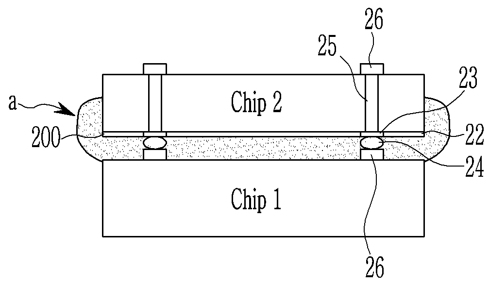
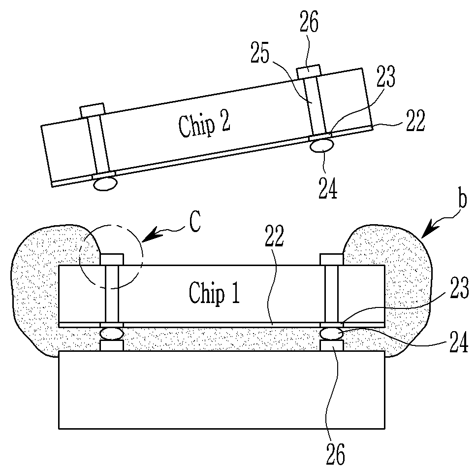
[0023]The substrate 10 may include a body part 21, a passivation layer 22, a lower pad 23, a connection member 24, a through-silicon via (TSV) 25, and an upper pad 26. The substrate 10 may be formed based on an active wafer and an interposer substrate. Herein, the active wafer means a wafer on which a semiconductor chip may be formed like a silicon wafer.

[0024]When the substrate 10 is formed based on the active wafer, the body part 21 may include a semiconductor substrate, an integrated circuit layer, an interlayer insulating layer, and an intermetallic ...


PUM


Abstract

A semiconductor package includes a semiconductor chip in which a side step or a side slope formed toward an inactive surface from an active surface is included and a width of the active surface is smaller than a width of the inactive surface, and an underfill which is disposed on the active surface and positioned at an inner side of the edge of the semiconductor chip.

Description

CROSS-REFERENCE TO RELATED APPLICATION[0001]This application claims priority from Korean Patent Application No. 10-2016-0169456 filed in the Korean Intellectual Property Office on Dec. 13, 2016, the entire contents of which are incorporated herein by reference.BACKGROUND OF THE INVENTIONField of the Invention[0002]Apparatuses and methods consistent with the present disclosure relate to a semiconductor package and a fabrication method thereof.Description of the Related Art[0003]In order to satisfy performance and cost required by consumers, integration of a semiconductor memory device needs to be increased. In the case of a two-dimensional (2D) or planar semiconductor memory device, the integration is mainly determined by an area occupied by a unit memory cell to be largely influenced by a level of a technique of forming minute patterns.[0004]For fineness of the patterns, since expensive equipment is required, integration of the 2D semiconductor memory device is limited. In order to ...

Claims


Application Information

Patent Timeline
Patent Type & Authority Applications(United States)
IPC IPC(8): H01L25/065H01L23/31H01L23/46
CPCH01L25/0657H01L23/3157H01L23/46H01L25/0652H01L23/3121H01L24/94H01L2225/06589H01L2225/06541H01L23/3128H01L23/473H01L2224/83005H01L2224/0401H01L2224/04105H01L2224/0557H01L2224/06181H01L2224/12105H01L2224/16145H01L2224/16227H01L2224/17181H01L2224/73204H01L2224/81005H01L2224/92125H01L2224/97H01L2225/1035H01L2225/1041H01L2225/1058H01L2924/15311H01L23/13H01L23/49816H01L2224/32145H01L2924/10156H01L2924/10155H01L2224/81H01L2224/83H01L2924/00012H01L23/562H01L21/563H01L23/31H01L24/81H01L24/10H01L2924/3511H01L2225/06513H01L2225/06555H01L29/06
Inventor PARK, SEUNG WONKO, YEONG KWON
Owner SAMSUNG ELECTRONICS CO LTD
Why Eureka
Try Eureka