Light emitting diode (LED) test apparatus and method of manufacture

Active Publication Date: 2018-06-21
APPLE INC
View PDF4 Cites 34 Cited by
  • Summary
  • Abstract
  • Description
  • Claims
  • Application Information

AI Technical Summary

Problems solved by technology

The device size and sheer volume of individual LED d

Method used


Image

  • Light emitting diode (LED) test apparatus and method of manufacture
  • Light emitting diode (LED) test apparatus and method of manufacture
  • Light emitting diode (LED) test apparatus and method of manufacture

Examples


embodiment 1700

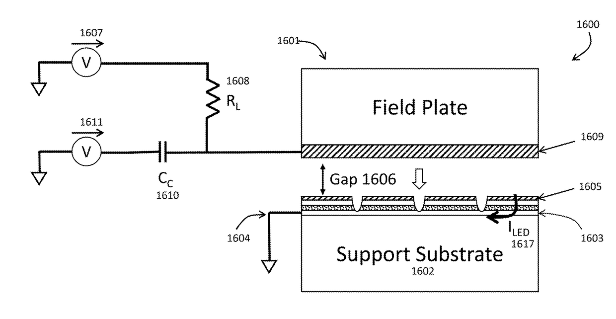
[0112]Although this invention has been described with a common contact existing under the LED devices, other configurations for injecting current are possible. FIG. 17A shows another embodiment 1700 where an analogue to the field plate 1701 is present within support substrate 1702 below the plurality of LED device structures such as LED device 1703. Under the lowest LED device structure layer (the n-layer in examples described in this invention), a dielectric layer 1704 and electrode 1705 completes the support substrate capacitive coupling device. Electrode 1705 is connected to a voltage source 1706. The field plate is connected to a separate voltage source 1707 and field plate electrode 1708. In this example, a camera 1709 is placed above the field plate to capture the light emission response of the plurality of LED devices under test. In this example, the isolation between devices is shown to be complete, however this method would still function with or without full isolation of t...

embodiment 1800

[0113]In yet another embodiment, C2I functional testing could also be applied to a modification of the test configuration of FIG. 17A that eliminates the need for a buried electrode within the support substrate. In this embodiment, the dielectric property of the support substrate itself is used to inject current through the LED devices. For example, a quartz, sapphire or plastic support substrate could serve as dielectric 1704 in FIG. 17A. FIG. 18 shows a specific embodiment 1800 of this configuration. A support substrate 1801 having adequate dielectric properties and thickness containing a plurality of LED devices on its surface such as LED device 1802 is placed on top of an electrode 1803 connected to a voltage source 1806. Field plate 1804 having a dielectric layer 1805 and electrode 1806 connected to a second voltage source 1807 completes the C2I functional test circuit. A camera 1808 placed above field plate 1804 is shown in this embodiment. The equivalent electrical circuit wo...


PUM


Abstract

Embodiments relate to functional test methods useful for fabricating products containing Light Emitting Diode (LED) structures. In particular, LED arrays are functionally tested by injecting current via a displacement current coupling device using a field plate comprising of an electrode and insulator placed in close proximity to the LED array. A controlled voltage waveform is then applied to the field plate electrode to excite the LED devices in parallel for high-throughput. A camera records the individual light emission resulting from the electrical excitation to yield a function test of a plurality of LED devices. Changing the voltage conditions can excite the LEDs at differing current density levels to functionally measure external quantum efficiency and other important device functional parameters.

Description

CROSS REFERENCE TO RELATED APPLICATION[0001]This application claims priority to U.S. Provisional Application No. 62 / 435,245, filed Dec. 16, 2016, commonly assigned and incorporated by reference herein for all purposes.FIELD OF INVENTION[0002]The present invention relates to light emitting diode (LED) devices. More particularly, embodiments of the invention relate to techniques, including methods and apparatus to functionally test a Light Emitting Diode (LED) array structure during the manufacturing process. In an example, the method is useful in general LED device functional testing and is particularly useful for functionally testing micro-LED (uLED) devices that can be as small as a few microns on a side. Micro-LEDs are grown on a support substrate utilizing techniques such as Metallo-Organic Chemical Vapor Deposition (MOCVD) among others. Before the individual devices are used in their final lighting or display application, it is desirable to test the LED devices to achieve one or...

Claims


Application Information

Patent Timeline
IPC IPC(8): H01L21/66H01L33/00H01L33/36H01L33/48
CPCH01L22/20H01L33/0095H01L33/36H01L33/48H01L2933/0016H01L2933/0033G01R31/2635G01R31/265G01R31/312G01R31/3025G09G3/006G01J1/42G09G3/3426G09G3/3413G09G2320/0242G09G3/32G01J2001/4252G01J1/46H01L22/34H01L22/14H01L21/67242
Inventor HENLEY, FRANCOIS J.
Owner APPLE INC
Why Eureka
Try Eureka