Semiconductor device and method for fabricating the same

a semiconductor device and semiconductor technology, applied in semiconductor devices, capacitors, electrical devices, etc., can solve problems such as the degraded reliability of semiconductor devices

Active Publication Date: 2018-06-21
SK HYNIX INC
View PDF3 Cites 18 Cited by
  • Summary
  • Abstract
  • Description
  • Claims
  • Application Information

AI Technical Summary

Benefits of technology

[0005]Embodiments of the present invention are directed to a semiconductor device which is substantially free of silicon dangling bonds in a memory cell region without deterioration of transistors in a peripheral circuit region, and a method for fabricating the semiconductor device.

Problems solved by technology

Thus, the reliability of a semiconductor device may be degraded.

Method used


Image

  • Semiconductor device and method for fabricating the same
  • Semiconductor device and method for fabricating the same
  • Semiconductor device and method for fabricating the same

Examples


first embodiment

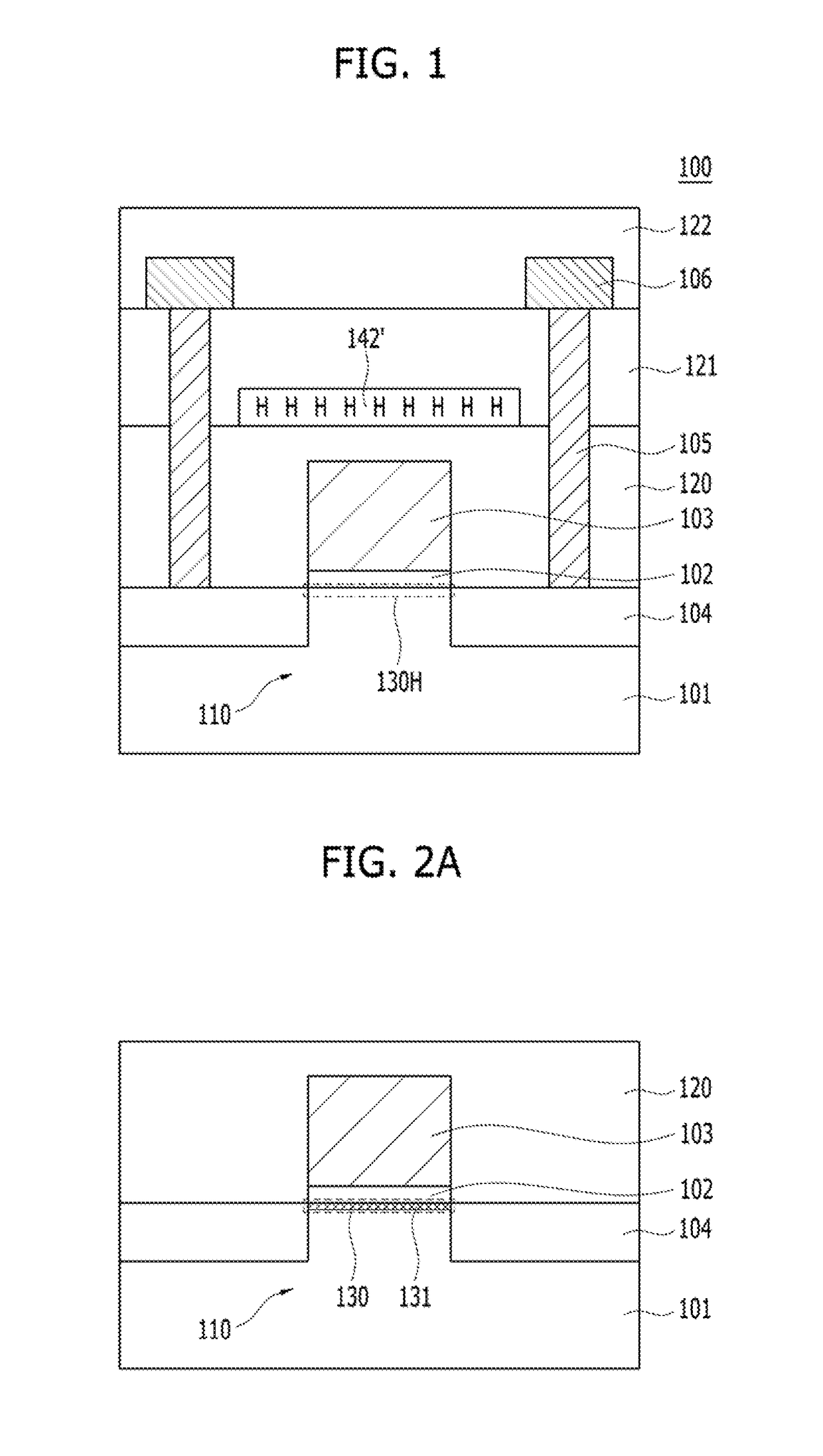
[0046]FIG. 1 is a cross-sectional view illustrating a semiconductor device 100 in accordance with the present invention.

[0047]Referring to FIG. 1, the semiconductor device 100 may include a transistor 110, and a hydrogen supplying layer 142′ formed over the transistor 110. The transistor 110 may include a substrate 101, a gate dielectric layer 102 disposed over the substrate 101, a gate electrode 103 disposed over the gate dielectric layer 102, a source / drain region 104 formed in the substrate 101. A first inter-layer dielectric layer 120 may be formed between the transistor 110 and the hydrogen supplying layer 142′. The semiconductor device 100 may further include a second inter-layer dielectric layer 121 covering the hydrogen supplying layer 142′ and the first inter-layer dielectric layer 120, and a third inter-layer dielectric layer 122 disposed over the second inter-layer dielectric layer 121. Also, the semiconductor device 100 may further include a metal line 106 contacting the...

second embodiment

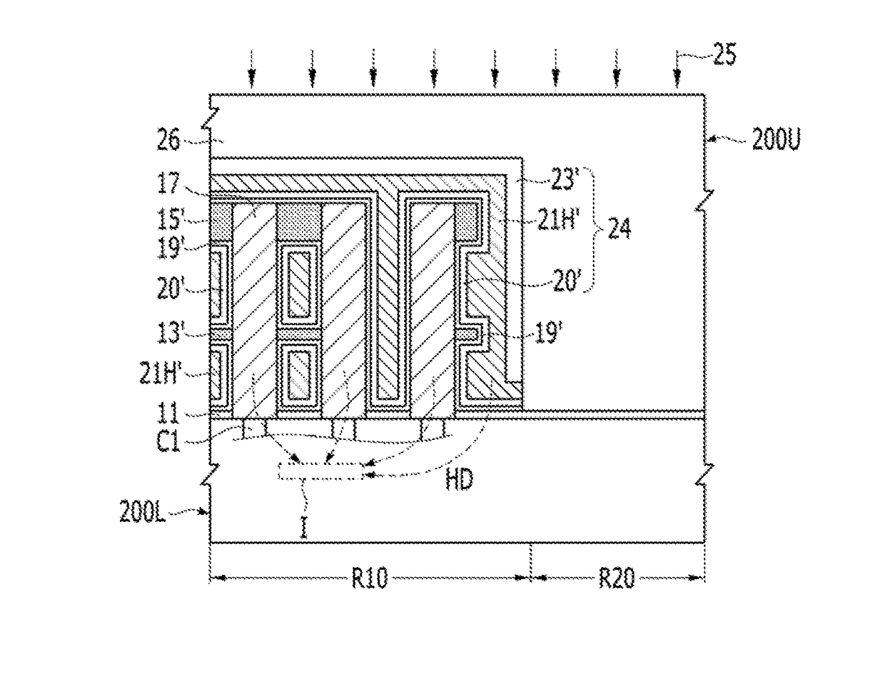
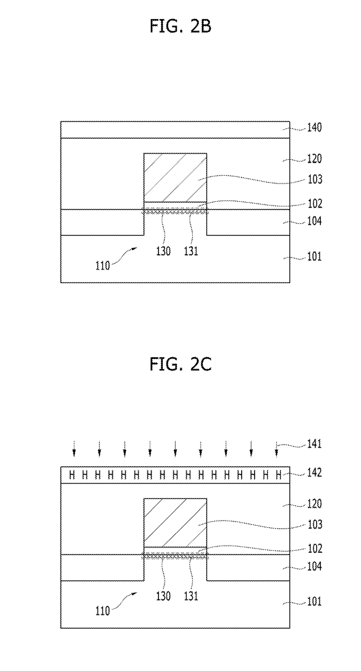
[0080]FIGS. 6A to 6J are cross-sectional views illustrating a method for fabricating the semiconductor device in accordance with the present invention. In a DRAM device, a peripheral circuit region for controlling data input and output to / from a memory cell may be generally provided, other than a cell region where memory cells are formed. When a plurality of constituent elements are formed in the cell region and the peripheral circuit region, some of the constituent elements may be formed to be concurrently merged.

[0081]Hereafter, for the sake of convenience in description, since the lower structure 200L disposed in the lower portion of the capacitor 310 among the constituent elements of the semiconductor device 200 shown in FIG. 3B may be manufactured by a well-known method, detailed explanation thereof will be omitted. The lower structure 200L may include an unpassivated interface I′ between the first gate dielectric layer 204 (see FIG. 3B) and the substrate 201 (see FIG. 3B). Her...


PUM

PropertyMeasurementUnit
aspect ratioaaaaaaaaaa
shapeaaaaaaaaaa
cylindrical shapeaaaaaaaaaa

Abstract

A method for fabricating a semiconductor device includes: forming a transistor in a semiconductor substrate; forming a capacitor including a hydrogen-containing top electrode over the transistor; and performing an annealing process for hydrogen passivation after the capacitor is formed.

Description

CROSS-REFERENCE TO RELATED APPLICATIONS[0001]The present application claims priority of Korean Patent Application No. 10-2016-0175505, filed on Dec. 21, 2016, which is incorporated herein by reference in its entirety.BACKGROUND1. Field[0002]Exemplary embodiments of the present invention relate to a semiconductor device and a method for fabricating the semiconductor device, and more particularly, to a semiconductor device including a capacitor and a method for fabricating the semiconductor device.2. Description of the Related Art[0003]Generally, a plurality of silicon dangling bonds are located at an interface between a silicon substrate and a gate dielectric layer in a Metal Oxide Silicon Field Effect Transistor (MOSFET) type semiconductor device. The silicon dangling bonds may function as interface traps to change a threshold voltage of the MOSFET. A characteristic of the MOSFET may be changed by the threshold voltage variation. Thus, the reliability of a semiconductor device may b...

Claims


Application Information

Patent Timeline
Patent Type & Authority Applications(United States)
IPC IPC(8): H01L27/108H01L49/02H01L21/321H01L21/3215H01L21/3213H01L21/3205H01L21/223
CPCH01L27/10852H01L28/75H01L21/321H01L21/3215H01L27/10885H01L21/32055H01L27/10876H01L27/10894H01L21/2236H01L21/32133H01L21/324H01L28/60H10B12/30H10B12/033H01L21/3003H10B12/34H10B12/315H10B12/053H01L28/82H01L21/02315H01L21/76801H01L21/76838H01L21/28255H10B12/31H10B12/09H10B12/482
Inventor JANG, IL-SIKPARK, JI-HWANLEE, MI-RIJEON, BONG-SEOKJOUNG, YONG-SOOHWANG, SUN-HWAN
Owner SK HYNIX INC
Why Eureka
Try Eureka