Micro-led module and method for fabricating the same

a micro-led module and micro-chip technology, applied in semiconductor/solid-state device manufacturing, electrical equipment, semiconductor devices, etc., can solve the problems of serious detection, large differences in expansion and contraction strains, and serious misalignment between the submount substrate and the micro-chip

Active Publication Date: 2018-06-28
LUMENS
View PDF4 Cites 9 Cited by
  • Summary
  • Abstract
  • Description
  • Claims
  • Application Information

AI Technical Summary

Benefits of technology

[0031]According to the present invention, the formation of the gap fill layer having a predetermined bonding strength between the submount substrate and the LED substrate can prevent the gap between the LED substrate and the submount substrate from becoming uneven from area to area at least after the micro-LED is mounted on the submount substrate. This enables the plurality of connection members, such as solder bumps, to more reliably connect the electrode pads of the micro-LED and the electrodes of the submount substrate.

Problems solved by technology

However, there are large differences in expansion and contraction strains between the Si-based submount substrate and the sapphire substrate upon heating and cooling during flip-bonding because the coefficient of thermal expansion of the Si-based submount substrate is significantly different from that of the sapphire substrate.
These differences cause a serious misalignment between the submount substrate and the micro-LED.
Due to this misalignment, the electrode pads of the micro-LED are not connected to the electrodes of the submount substrate, and in a more severe case, the electrode pads of the micro-LED are misconnected to the electrodes of the submount substrate, causing serious detects, such as electrical shorting.
In this case, the large difference in coefficient of thermal expansion between the sapphire substrate and the submount substrate causes a misalignment between the micro-LED and the submount substrate, making it difficult to bond the micro-LED to the submount substrate.
For example, when the melting point (260° C.) of the solder is set as a bonding temperature, an misalignment of 5 to 6 μm is caused per 1 cm of the substrates, making it substantially impossible to use the solder in a process where a bonding precision of 2 μm is required, like flip-bonding of the micro-LED.
For a display with a lower precision of ≤2 μm, it is not easy to bond an LED substrate made of sapphire to a Si-based submount substrate due to their different coefficients of thermal expansion.
This heating further increases the difference in strain resulting from different coefficients of thermal expansion of the LED substrate and the submount substrate, making it substantially impossible to bond the LED substrate to the submount substrate.
Indium as a solder material with a relatively low melting point can be used for bonding but misalignment is inevitable.
Even when misalignment is reduced by decreasing the difference in strain caused by different coefficients of thermal expansion of an LED substrate and a submount substrate of a micro-LED, a slight gap may exist from area to area between the LED substrate and the submount substrate, resulting in loss of the function of connection members to connect electrode pads of the micro-LED to electrodes of the submount substrate.
Particularly, the larger the difference in coefficient of thermal expansion between the LED substrate and the submount substrate, the more uneven the gap between the LED substrate and the submount substrate, making the above problem worse.

Method used


Image

  • Micro-led module and method for fabricating the same
  • Micro-led module and method for fabricating the same
  • Micro-led module and method for fabricating the same

Examples


first embodiment

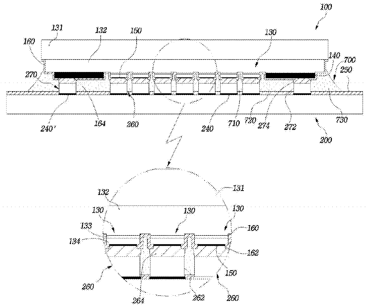
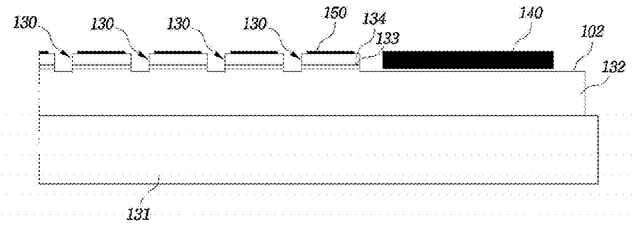
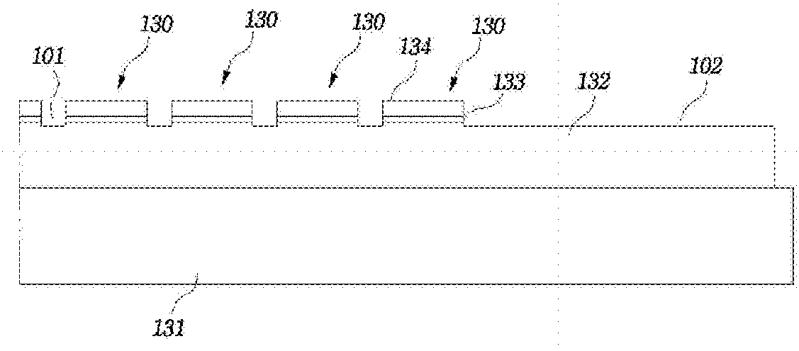
[0054]Referring to FIG. 1, a micro-LED module according to a first embodiment of the present invention includes at least one micro-LED 100 including a plurality of LED cells 130 arrayed in a matrix and a submount substrate 200 mounted with the micro-LED 100. The micro-LED 100 includes at least one common electrode pad 140 disposed in an area corresponding to the peripheral edge thereof. A plurality of individual electrode pads 150 are disposed on the micro-LED 100 so as to correspond to the LED cells 130 arrayed in a matrix. The submount substrate 200 includes pad-type electrodes 240 and 240′ formed corresponding to the common electrode pad 140 and the individual electrode pads 150, respectively. As used herein, the term “individual electrode pad” means an electrode pad individually connected to an n-type semiconductor layer or a p-type semiconductor layer provided in one LED cell. As used herein, the term “common electrode pad” means an electrode pad connected in common to n-type o...

second embodiment

[0114]Referring to FIG. 10, a micro-LED module according to a second embodiment of the present invention includes at least one micro-LED 100 including a plurality of LED cells 130 arrayed in a matrix and a submount substrate 200 mounted with the micro-LED 100. The micro-LED module includes a plurality of electrode pads 140 and 150 provided in the micro-LED 100 and pad-type electrodes 240 and 240′ formed corresponding to the plurality of electrode pads 140 and 150 in the submount substrate 200. The micro-LED 100 includes connection members through which the electrode pads 140 and 150 are connected to the electrodes 240 and 240′ at room temperature without the need to use solders requiring high-temperature melting. Each of the connection members includes a conductive soft block 2 and a conductive insert rod 3 embedded in and electrically connected to the conductive soft block 2 by a vertical force, i.e. a vertical compressive force.

[0115]In the micro-LED 100, one n-type semiconductor ...

third embodiment

[0141]According to a general flip-bonding process for mounting a micro-LED, as the size of solder bumps decreases, the current density and thermal energy density per bump connecting portion increases, resulting in a reduction in the reliability of the flip solder connecting portion. Fine intervals between adjacent solder bumps increase the risk that solder bridging with other adjacent solder bumps may occur upon solder reflow.

[0142]The above problem is solved by a flip-bonding technique using Cu pillar bumps. The use of Cu pillar bumps enables much finer flip-bonding without a reduction in the distance between LED cells and an active matrix substrate. Another advantage of flip-bonding is that the electrical and thermal properties of a micro-LED can be improved because the electrical and thermal conductivities of Cu are much higher than those of solder alloys.

[0143]However, this method suffers from difficulty in terms of process control when an under bump metallurgy (UBM) is formed o...


PUM


Abstract

A micro-LED module is disclosed. The micro-LED module includes: a micro-LED including a plurality of LED cells, each of which includes a first conductive semiconductor layer, an active layer, and a second conductive semiconductor layer; a submount substrate mounted with the micro-LED; a plurality of electrode pads formed on the micro-LED cells; a plurality of electrodes formed corresponding to the plurality of electrode pads on the submount substrate; a plurality of connection members through which the plurality of electrode pads are connected to the corresponding plurality of electrodes; and a gap fill layer formed in the gap between the micro-LED and the submount substrate and having a bonding strength to the micro-LED and the submount substrate.

Description

BACKGROUND OF THE INVENTION1. Field of the Invention[0001]The present invention relates to a micro-LED module including a micro-LED and a submount substrate mounted with the micro-LED. More specifically, the present invention relates to a micro-LED module in which the gap between a micro-LED and a submount substrate is prevented from becoming uneven from area to area so that connection members can be prevented from losing their function to connect electrode pads of the micro-LED to electrodes of the submount substrate, and a method for fabricating the micro-LED module.2. Description of the Related Art[0002]Displays using micro-LED modules are known. Each of the micro-LED modules is fabricated by flip-bonding a micro-LED including a plurality of LED cells to a submount substrate.[0003]The micro-LED includes a light-transmitting sapphire substrate and a gallium nitride semiconductor light emitting unit formed on the light-transmitting sapphire substrate and having a plurality of LED c...

Claims


Application Information

Patent Timeline
Patent Type & Authority Applications(United States)
IPC IPC(8): H01L25/075H01L33/54H01L33/62H01L33/36H01L25/00
CPCH01L25/0753H01L33/54H01L33/62H01L33/36H01L25/50H01L27/156H01L33/0095H01L2933/005H01L2224/11H01L2224/13082H01L33/08H01L2224/86203H01L21/447H10K59/00H10K59/10H10K59/90
Inventor KIM, DAEWONSHIN, EUNSUNGMOON, MYUNGJICHANG, HANBEETKIM, YONGPILPARK, JAESOON
Owner LUMENS
Why Eureka
Try Eureka