Standard cell architecture with at least one gate contact over an active area

Active Publication Date: 2018-07-26
IBM CORP
View PDF11 Cites 6 Cited by
  • Summary
  • Abstract
  • Description
  • Claims
  • Application Information

AI Technical Summary

Benefits of technology

[0010]The advantages include leveraging gate contacts over active regions to reduce a number of metal layers used while improving pin access and supporting a shortened cell height. Additional advantages include maximizing effective device width (i.e., number of fins) to improve device performance (i.e., by having more active fins). Further advantages inc

Problems solved by technology

Standard semiconductor cell library performance is limited by the current a transistor of a cell can deliver.
The devices also exhibit wide performance differences due to semiconductor process variations.
However, this approach produces additional disadvantages.
This known prior art approach increases the parasitic coupling significantly, thereby slowing down circuit performance.
The amount of silicon needed to implement the cells increases as

Method used


Image

  • Standard cell architecture with at least one gate contact over an active area
  • Standard cell architecture with at least one gate contact over an active area
  • Standard cell architecture with at least one gate contact over an active area

Examples


Embodiment Construction

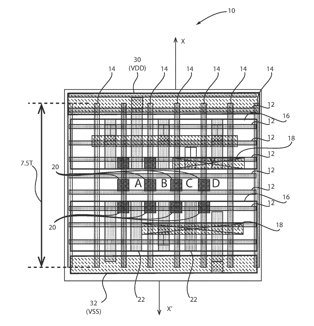
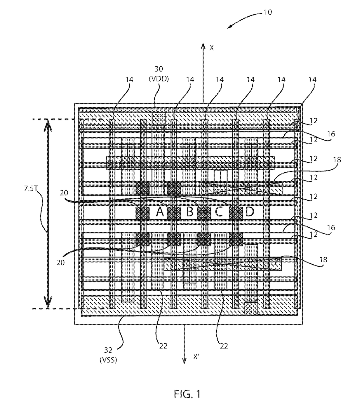
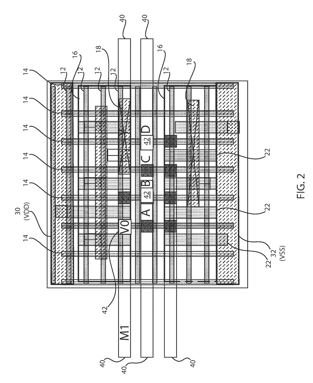
[0031]In accordance with an embodiment, a method is provided for forming a layout of a standard cell. The method includes forming a plurality of gate conductors, forming a plurality of active areas, and forming at least one gate contact (CB contact) within an active region of the plurality of active regions.

[0032]In accordance with another embodiment, a layout of a standard cell is provided. The layout of the standard cell includes a plurality of gate conductors, a plurality of active areas, and at least one gate contact (CB contact) formed within an active region of the plurality of active regions.

[0033]In one or more embodiments, a new and useful logic standard cell architecture is presented that advantageously leverages gate contacts over active regions to reduce the number of metals used while improving pin access. In addition, effective device width (i.e., number of fins) can be maximized to improve performance. AUXFIN is also introduced as a complete and useful design solution...


PUM


Abstract

A method is presented for forming a layout of a MOSFET (metal oxide semiconductor field effect transistor) circuit. The method includes forming a plurality of gate conductors, forming a plurality of active areas, and forming at least one gate contact (CB contact) within an active region of the plurality of active regions. The method further includes placing a marker over the at least one gate contact to identify a location of the at least one gate contact. Additionally, a distance between the at least one gate contact and at least one TS contact is optimized based on device specifications.

Description


Claims


Application Information

Patent Timeline
IPC IPC(8): H01L27/02G06F17/50
CPCH01L27/0207G06F17/5077G06F17/5072G06F30/39G06F30/392H01L27/11807H01L2027/11866G06F30/394
Inventor CHU, ALBERT M.NA, MYUNG-HEERAMACHANDRAN, RAVIKUMAR
Owner IBM CORP
Why Eureka
Try Eureka