OLED display and manufacturing method thereof

a technology of light-emitting diodes and oled panels, which is applied in the direction of basic electric elements, electrical apparatus, and semiconductor devices, etc., can solve the problems of deterioration of the performance of the oled device closely related to material degradation, and the process is not suitable for flexible devices, so as to reduce the thermal decomposition of materials, prolong the service life of the device, and effectively transfer heat

Active Publication Date: 2018-07-26
WUHAN CHINA STAR OPTOELECTRONICS TECH CO LTD
View PDF4 Cites 8 Cited by
  • Summary
  • Abstract
  • Description
  • Claims
  • Application Information

AI Technical Summary

Benefits of technology

[0008]An objective of the present invention is to provide an organic light-emitting diode (OLED) display, which allows for effective transfer of heat generated during an operation of an OLED device, reduces thermal decomposition of a material of the OLED device, and extends the service life of the device while ensuring sufficient capability of the device in blocking external moisture and oxygen.
[0009]Another objective of the present invention is to provide a manufacturing method of an OLED display, which includes a patterned layer of high thermal conductivity in a thin film encapsulation structure to provide effective transfer of heat generated during an operation of an OLED device, reduce thermal decomposition of a material of the OLED device, and extend the service life of the device while ensuring sufficient capability of the device in blocking external moisture and oxygen.
[0042]The efficacy of the present invention is that the present invention provides an OLED display, which comprises an OLED substrate and a thin film encapsulation layer disposed on the OLED substrate, wherein the thin film encapsulation layer comprises a patterned the high thermal conductivity layer and the high thermal conductivity layer is provided with a plurality of openings formed therein to correspond, in a one to one manner, to a plurality of sub-pixel areas of the OLED substrate so as to prevent the high thermal conductivity layer from absorbing light and also help eliminate the constraint that a top emission device is only allowed to use a material having a high transmission rate, thereby allowing for effective transfer of heat generated during an operation of an OLED device without deteriorating light emission efficiency of the device, reducing thermal decomposition of a material of the OLED device, and ensuring the device possesses sufficiency capability of blocking external moisture and oxygen to thus extend the service life of the device; and the present invention provides a manufacturing method of an OLED display, which adopts thin film encapsulation to package an OLED device and adds a patterned high thermal conductivity layer in the thin film encapsulation structure, wherein the high thermal conductivity layer is provided with a plurality of openings formed therein to correspond, in a one to one manner, to a plurality of sub-pixel areas of the OLED substrate so as to prevent the high thermal conductivity layer from absorbing light and also help eliminate the constraint that a top emission device is only allowed to use a material having a high transmission rate, thereby allowing for effective transfer of heat generated during an operation of an OLED device without deteriorating light emission efficiency of the device, reducing thermal decomposition of a material of the OLED device, and ensuring the device possesses sufficiency capability of blocking external moisture and oxygen to thus extend the service life of the device.

Problems solved by technology

However, the organic material is susceptible to reaction with moisture and oxygen and thus, a display based that is based on the organic material is subject to extremely severe requirement for packaging of an OLED display panel.
Such processes are not fit for flexible devices.
On the other hand, massive results of study and research reveal deterioration of the performance of an OLED device is closely related to material degradation resulting from heat generated by the device itself.
However, it is known that such packaging techniques involve inorganic metal oxides and organic materials, of which thermal conductivity is generally poor, making it hard to conduct away heat generated by a device.
However, the transmission rate of Cu is not high enough, and, particularly for application in a top emission device in the display field, such a technique is subjected great limitation.
However, covering Ag on an entire surface of the thin film in a top emission device would reduce outward emission of light so that such a heat conducting material suffers certain limitations.

Method used


Image

  • OLED display and manufacturing method thereof
  • OLED display and manufacturing method thereof
  • OLED display and manufacturing method thereof

Examples


Embodiment Construction

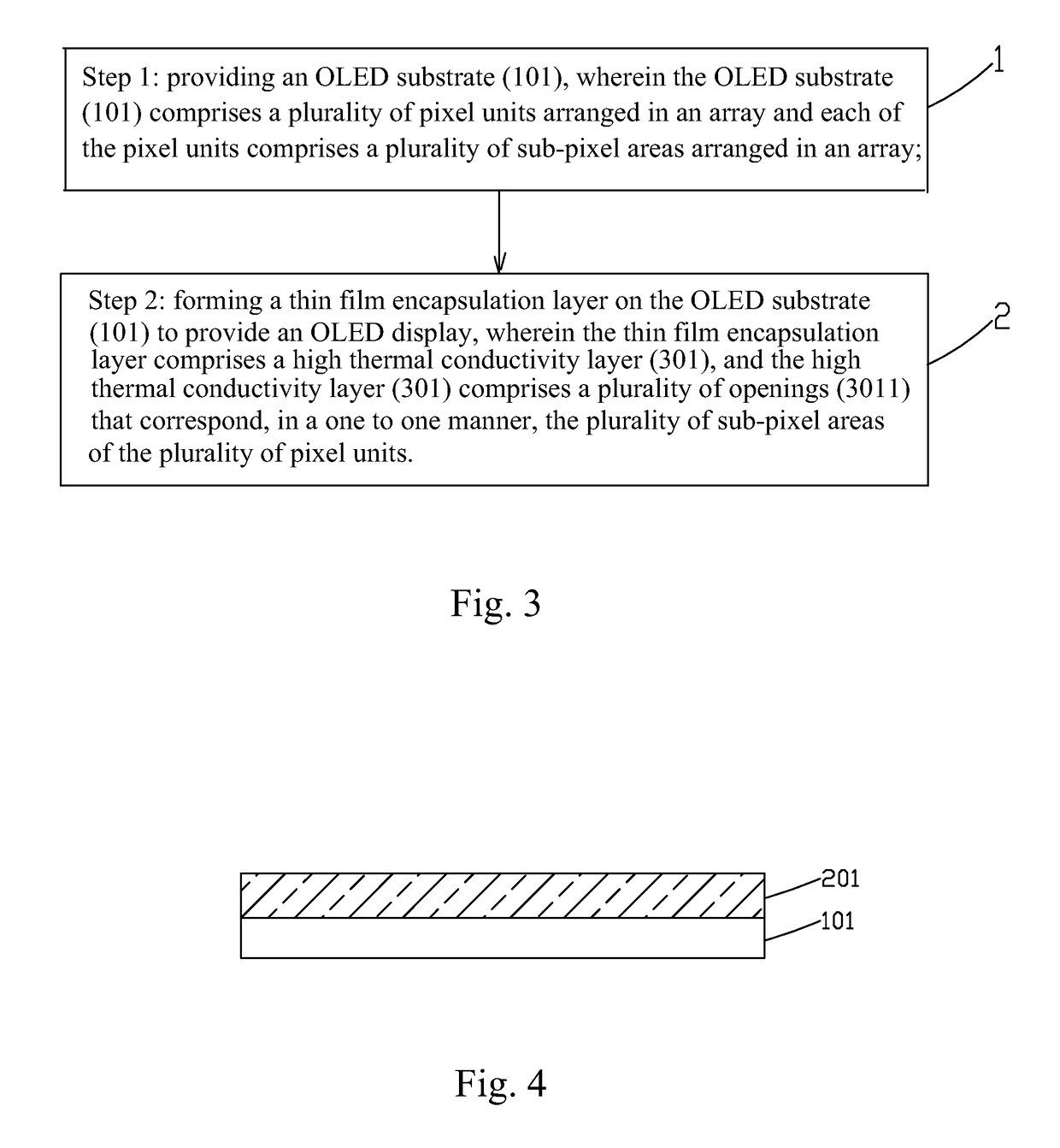
[0053]To further expound the technical solution adopted in the present invention and the advantages thereof, a detailed description will be given with reference to the preferred embodiments of the present invention and the drawings thereof.

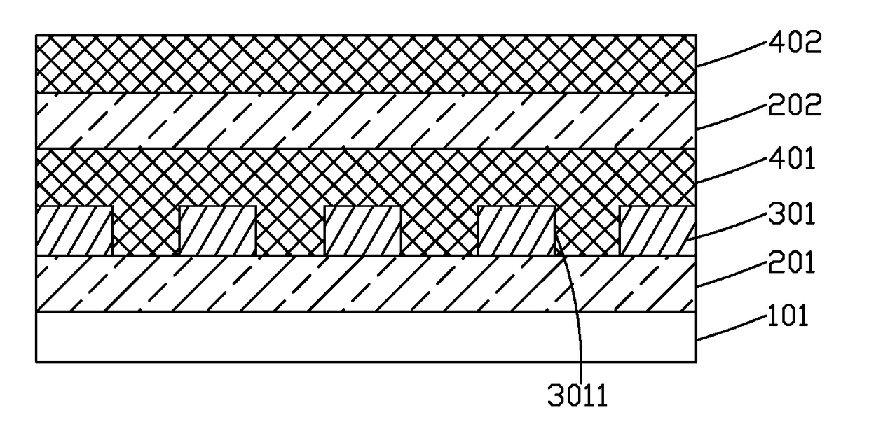
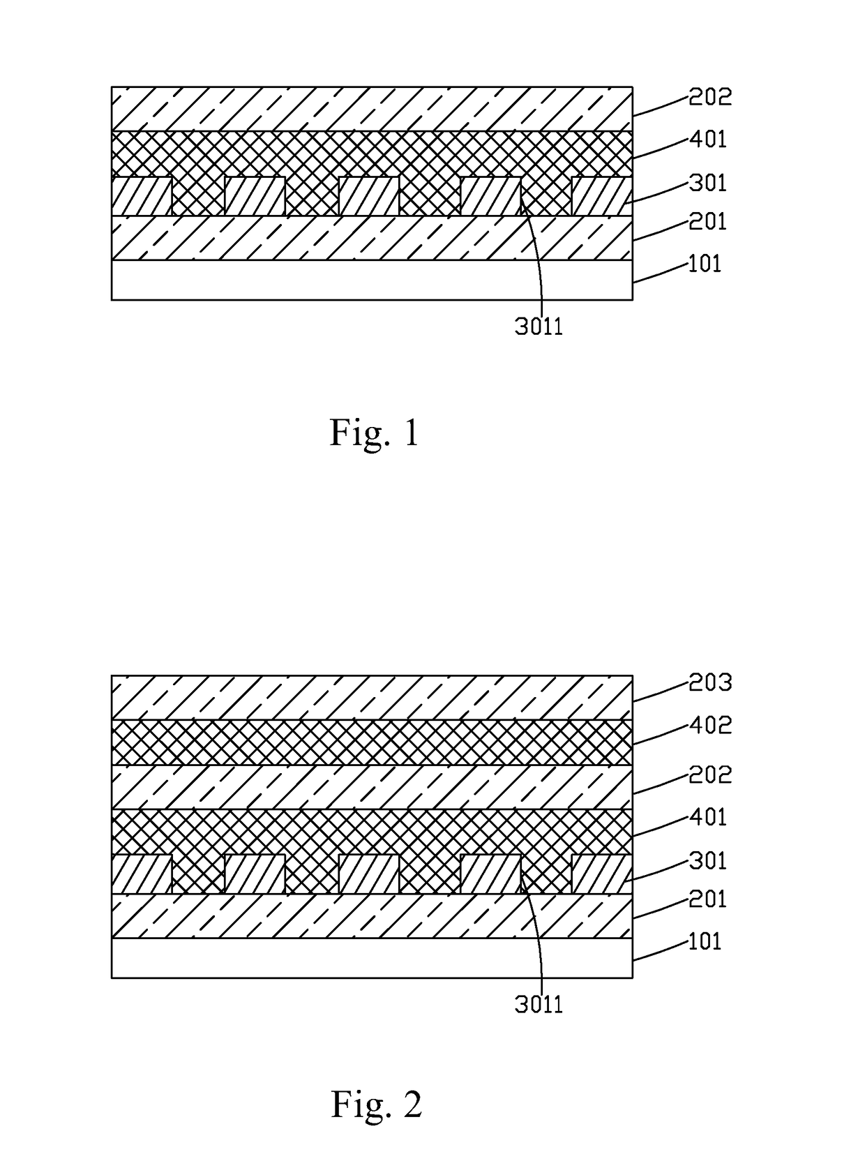
[0054]Referring to FIG. 1, which is a schematic view showing the structure of a first embodiment of an organic light-emitting diode (OLED) display according to the present invention, in the instant embodiment, the OLED display comprises an OLED substrate 101 and a thin film encapsulation layer disposed on the OLED substrate 101.

[0055]The thin film encapsulation layer comprises a first inorganic passivation layer 201 disposed on the OLED substrate 101, a high thermal conductivity layer 301 disposed on the first inorganic passivation layer 201, a first organic buffer layer 401 disposed on the first inorganic passivation layer 201 and the high thermal conductivity layer 301, and a second inorganic passivation layer 202 disposed on the first organic b...


PUM

PropertyMeasurementUnit
thicknessaaaaaaaaaa
thicknessaaaaaaaaaa
thicknessaaaaaaaaaa

Abstract

The present invention provides an OLED display and a manufacturing method thereof. The OLED display of the present invention includes an OLED substrate and a thin film encapsulation layer disposed on the OLED substrate. The thin film encapsulation layer includes a patterned the high thermal conductivity layer and the high thermal conductivity layer is provided with a plurality of openings formed therein to correspond, in a one to one manner, to a plurality of sub-pixel areas of the OLED substrate so as to prevent the high thermal conductivity layer from absorbing light and also help eliminate the constraint that a top emission device is only allowed to use a material having a high transmission rate, thereby allowing for effective transfer of heat generated during an operation of an OLED device without deteriorating light emission efficiency of the device, reducing thermal decomposition of a material of the OLED device, and ensuring the device possesses sufficiency capability of blocking external moisture and oxygen to thus extend the service life of the device.

Description

BACKGROUND OF THE INVENTION1. Field of the Invention[0001]The present invention relates to the field of flat panel display technology and more particular to an organic light-emitting diode (OLED) display and a manufacturing method thereof.2. The Related Arts[0002]OLED displays possess advantages, such as being self-luminous, high brightness, wide view angle, high contrast, being flexible, and low power consumption, and thus attract much attention as a new generation of displaying solution that gradually takes the place of traditional liquid crystal displays. It is now a symbol of being high tech by adopting an OLED display panel from small size ones used in mobile phone display screens to large size ones used in high definition flat panel televisions.[0003]The OLED based display technology is different from the traditional liquid crystal display technology in that no backlighting is necessary and an extremely thin organic material coating layer and a glass substrate are involved so ...

Claims


Application Information

Patent Timeline
Patent Type & Authority Applications(United States)
IPC IPC(8): H01L51/52H01L27/32H01L51/56
CPCH01L51/5256H01L51/56H01L27/3213H01L27/1259H01L27/1214H01L51/5253H01L27/1251H01L51/5296H01L51/5237H01L27/1248H01L25/0753H10K59/00H10K59/122H10K50/8445H10K50/844H10K50/84H10K71/00H10K59/351H10K50/87H10K2102/00H10K50/30
Inventor JIN, JIANGJIANG
Owner WUHAN CHINA STAR OPTOELECTRONICS TECH CO LTD
Why Eureka
Try Eureka