SYSTEM AND METHOD FOR DESIGNING SYSTEM ON CHIP (SoC) CIRCUITS USING SINGLE INSTRUCTION MULTIPLE AGENT (SIMA) INSTRUCTIONS

a technology of instruction and instruction, applied in the field of apparatus/systems for designing integrated circuits, can solve the problems of not having a system and method, design does not teach about implementing an ai framework, and the process of converting a design flow (of a soc circuit) into a physical design is not free from (design related) errors

Active Publication Date: 2018-09-13
ALPHAICS CORP
View PDF2 Cites 21 Cited by
  • Summary
  • Abstract
  • Description
  • Claims
  • Application Information

AI Technical Summary

Problems solved by technology

Further, the process of converting a design flow (of a SoC circuit) into a physical design is not free from (design related) errors due to a manual implementation and fragmented nature (of the corresponding design flow).
Typically, functional verification (for determining whether the logic design of the SoC circuit confirms to the design specification), which forms a critical part of the transformation from design flow (of a SoC circuit) to physical design, demands the largest pool of resources (in terms of time, manpower inter-alia), due to the complexity of the SoC circuit, design as well as the enormity of possible test cases / test scenarios necessary to completely verify the SoC circuit design in its entirety.
At present, there is no system and method available and exist for generalization and learnability of data generated in chip designing process.
The existing process of SoC chip design does not teach about implementing an AI framework into the manual chip design process.
The advanced AI based framework for chip design is not supported by general purpose computer based on RISC and GPGPU and even FPGAs.
Further, existing hardware do not provide Application specific instructions configured to perform SoC chip design.

Method used


Image

  • SYSTEM AND METHOD FOR DESIGNING SYSTEM ON CHIP (SoC) CIRCUITS USING SINGLE INSTRUCTION MULTIPLE AGENT (SIMA) INSTRUCTIONS
  • SYSTEM AND METHOD FOR DESIGNING SYSTEM ON CHIP (SoC) CIRCUITS USING SINGLE INSTRUCTION MULTIPLE AGENT (SIMA) INSTRUCTIONS
  • SYSTEM AND METHOD FOR DESIGNING SYSTEM ON CHIP (SoC) CIRCUITS USING SINGLE INSTRUCTION MULTIPLE AGENT (SIMA) INSTRUCTIONS

Examples


Embodiment Construction

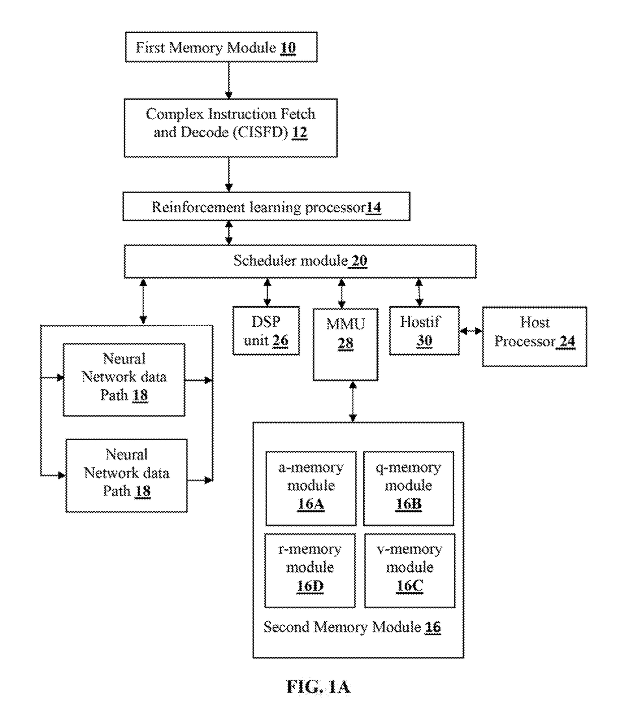
[0011]An object of the embodiments herein is to provide a system with AI processor implementing SoC design framework.

[0012]Another object of the embodiments herein is to provide a system with application specific instructions or Single Instruction Multiple Agent instructions for designing SoC.

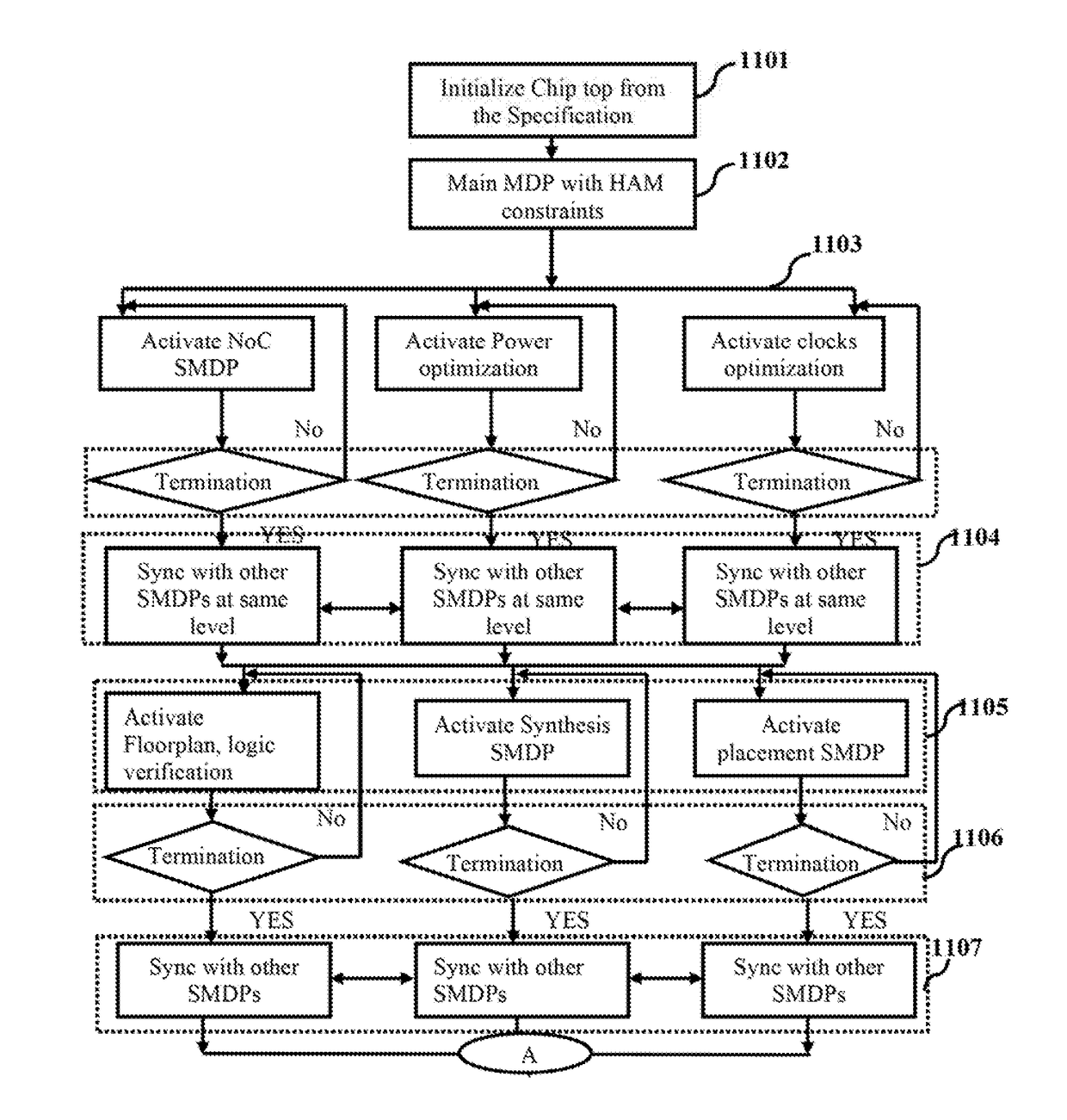
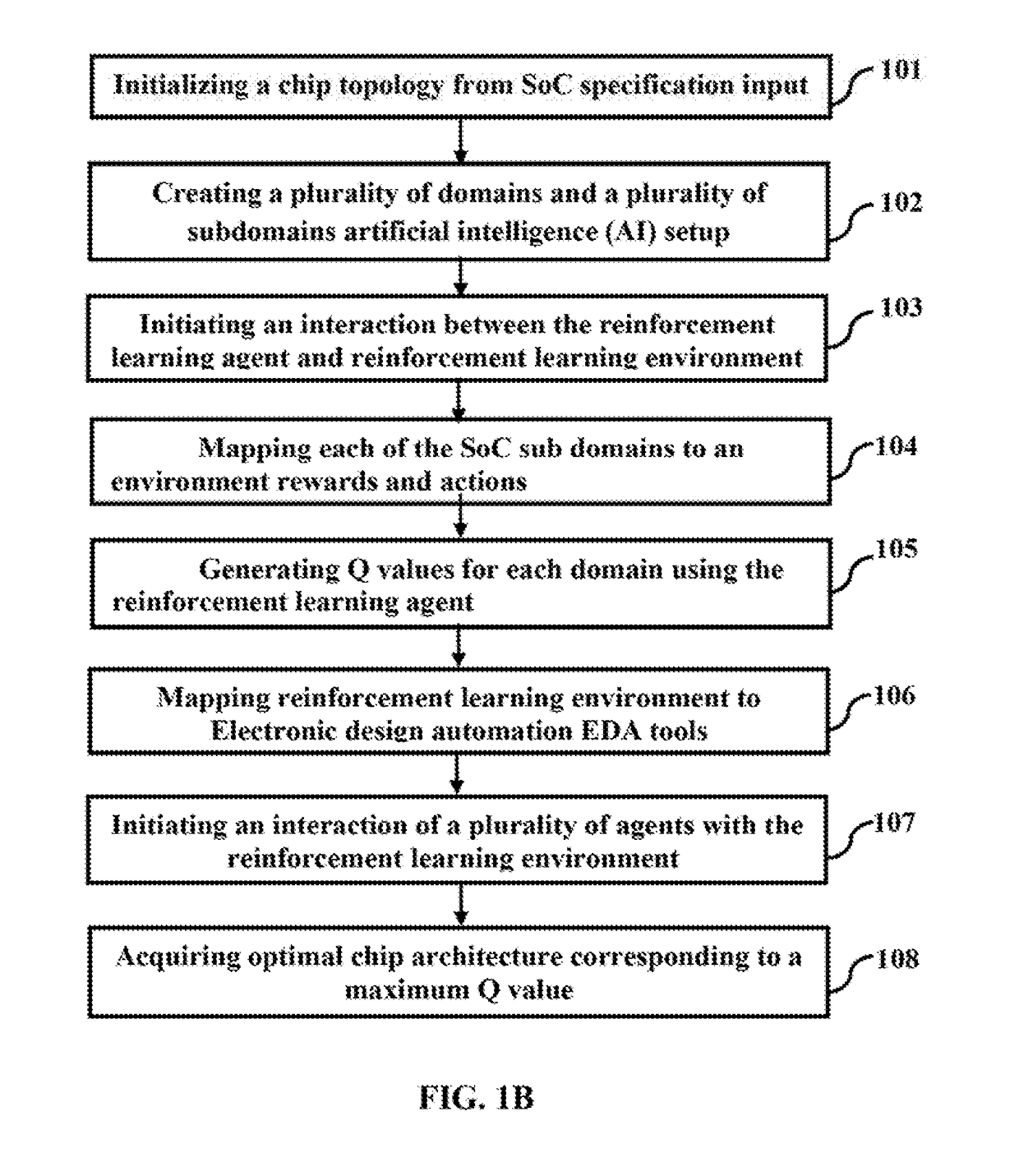
[0013]Yet another object of the embodiments herein SoC design framework that employs reinforcement learning techniques to improve the design and implementation of SoC circuit design,

[0014]Yet another object of the embodiments herein is to provide an artificial intelligence based framework optimized for SoC design and implementation.

[0015]Yet another object of the embodiments herein is to provide a method for learning and inferencing from SoC design that can be used for future designing of SoC.

[0016]Yet another object of the embodiments herein is to provide a SoC design framework that automates the process of SoC design and implementation,

[0017]Yet another object of the embodiments herein is to ...


PUM


Abstract

The embodiments herein discloses a system and method for designing SoC by using a reinforcement learning processor. An SoC specification input is received and a plurality of domains and a plurality of subdomains is created using application specific instruction set to generate chip specific graph library. An interaction is initiated between the reinforcement learning agent and the reinforcement learning environ lent using the application specific instructions. Each of the SoC sub domains from the plurality of SoC sub domains is mapped to a combination of environment, rewards and actions by a second processor. Further, interaction of a plurality of agents is initiated with the reinforcement learning environment for a predefined number of times and further Q value, V value, R value, and A value is updated in the second memory module. Thereby, an optimal chip architecture for designing SoC is acquired using application-domain specific instruction set (ASI).

Description

CROSS-REFERENCE TO RELATED APPLICATION[0001]This application is a continuation-in-part of the divisional application with the Ser. No. 15 / 697,803 filed on Sep. 7, 2017 with the tide “SYSTEM AND METHOD FOR DESIGNING SYSTEM ON CHIP (SoC) CIRCUITS BY SYNCHRONIZING A HIERARCHY OF SMDPs” and claims priority from U.S. Non-Provisional patent application Ser. No. 15 / 455,126, filed on Mar. 9, 2017, entitled “PROCESSOR FOR IMPLEMENTING REINFORCEMENT LEARNING OPERATIONS” and also claims the priority of the U.S. Non-Provisional patent application Ser. No. 15 / 499,832, filed on Apr. 27, 2017, with the title “SYSTEM AND METHOD FOR DESIGNING SYSTEM ON CHIP (SoC) CIRCUITS THROUGH ARTIFICIAL INTELLIGENCE AND REINFORCEMENT LEARNING”, The contents of abovementioned applications are included entirely as reference herein.BACKGROUNDTechnical Field[0002]The embodiments herein is related to apparatuses / systems for designing Integrated Circuits (IC). The embodiments herein is particularly related to apparatu...

Claims


Application Information

Patent Timeline
Patent Type & Authority Applications(United States)
IPC IPC(8): G06F17/50
CPCG06F17/505G06F17/504G06F30/327G06F30/3323
Inventor NAGARAJA, NAGENDRA
Owner ALPHAICS CORP
Why Eureka
Try Eureka