Semiconductor integrated circuit with guard ring

a technology of integrated circuits and shield rings, applied in the direction of basic electric elements, semiconductor devices, electrical equipment, etc., can solve the problems of increased device size, reduced gain of parasitic bipolar devices, and increased risk of weak spots, so as to reduce the risk of weak spots

Active Publication Date: 2018-09-27
RENESAS ELECTRONICS CORP
View PDF1 Cites 8 Cited by
  • Summary
  • Abstract
  • Description
  • Claims
  • Application Information

AI Technical Summary

Benefits of technology

The power protection circuit described in this patent prevents damage to sensitive components in a semiconductor integrated circuit caused by surge voltage pulses. It uses a third diode to protect the MOS transistors in the output buffer. This circuit design reduces the risk of destruction of the sensitive components in the junction between the protection device and the guard ring region.

Problems solved by technology

As a result, the base region of the parasitic bipolar device is widened and the gain of the parasitic bipolar device decreases, such that the parasitic bipolar device is hard to be operated.
The inter-power source clamp circuit 15 has a problem in that there is the limiting characteristic of arrangement dependency, and the device size increases.
Meanwhile, when the arrangement location of the inter-power source clamp circuit 15 is not appropriate, with the addition of the parasitic factors, such as power interconnect resistance, overall impedance of the inter-power source clamp circuit 15 when viewed from an external terminal may increase, and another device may be unintentionally turned on antecedently and may discharge a surge.
In the case of an internal circuit in which the device is miniaturized, device destruction occurs.
As a result, with the arrangement of the inter-power source clamp circuits 15, the influence on a semiconductor chip area is unavoidable.
With the layout restriction to the arrangement of other circuit blocks or the arrangement of power interconnects, there is a case where it is difficult to arrange the inter-power source clamp circuit 15.
As described above, if the operation start time until the bypass device between the power sources through the output buffer 14 operates is delayed, the PN junction between the P-type impurity layer and the N-type well region N-Well of the first diode D1 to which a reverse bias is applied becomes a weak spot (Wk_Sp1) , causing an increased risk of junction destruction.
Similarly, the PN junction (parasitic diode D4) between the N-type well region N-Well of the first diode D1 and the P-type well region P-Well of the second diode D2 to which a reverse bias is applied becomes a weak spot (Wk_Sp2), causing an increased risk of junction destruction.
According to this method, however, the device size of the parasitic diode D4 simply increases and inevitably affects the chip area, causing a problem in the reduction in device size.
In regard to the power source clamp circuit 15, as described above, since the arrangement itself of the power source clamp circuit 15 considerably affects the chip size, there is also a problem in the reduction in device size.
As a result, the short side portion of the N-type impurity region of the cathode K formed in the longitudinal rectangular shape becomes the weak spot Wk_Sp, and the current density of the surge discharge current becomes higher, causing destruction.

Method used


Image

  • Semiconductor integrated circuit with guard ring
  • Semiconductor integrated circuit with guard ring
  • Semiconductor integrated circuit with guard ring

Examples


embodiment 1

>

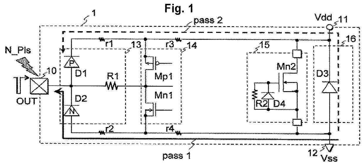
[0234]FIG. 1 is a diagram showing the configuration of a semiconductor integrated circuit equipped with an electrostatic protection circuit (ESD protection circuit) according to Embodiment 1 of the invention.

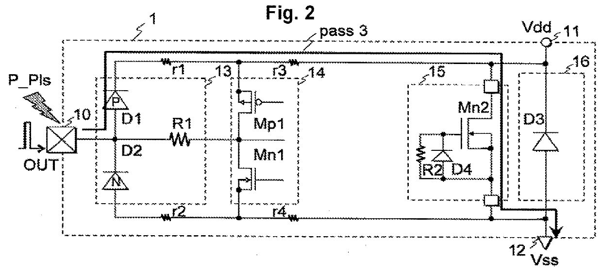
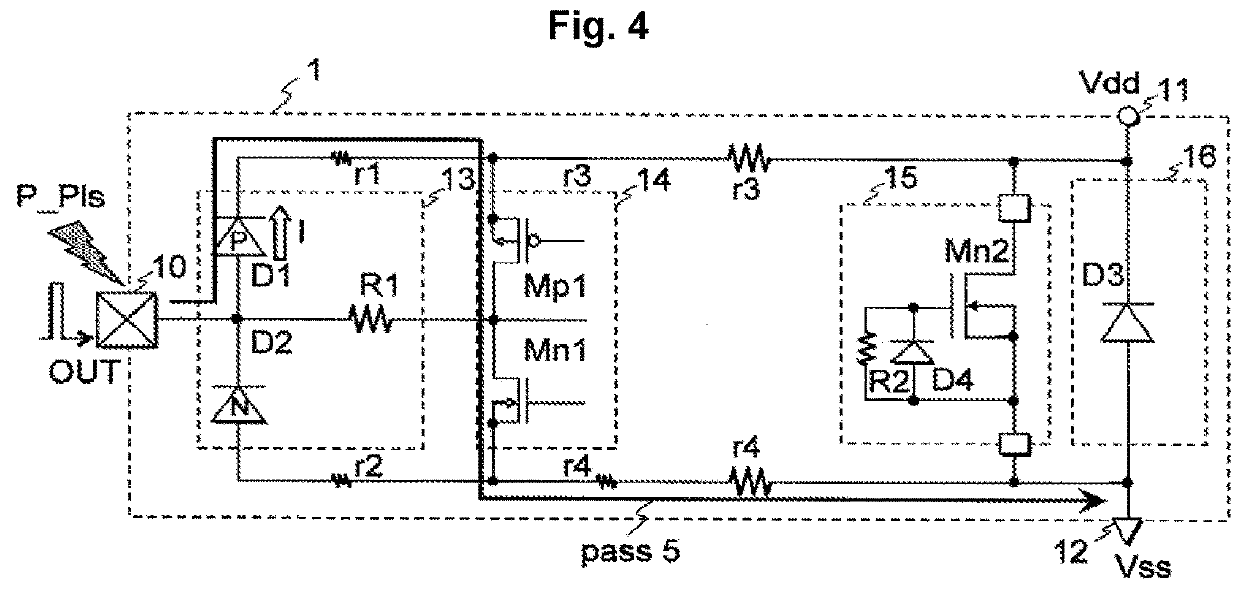
[0235]The semiconductor integrated circuit 1 shown in FIG. 1 includes an output terminal 10, an electrostatic protection circuit 13, an output buffer 14, an inter-power source clamp circuit 15, a power protection circuit 16, a power supply terminal 11, and a ground terminal 12. Resistors r1, r2, r3, and r4 are interconnect resistance. >

[0236]The output buffer 14 includes a P-channel MOS transistor Mp1 and an N-channel MOS transistor Mn1 connected in series between the power supply terminal 11 and the ground terminal 12. The driving output signals of the drain of the P-channel MOS transistor Mp1 and the drain of the N-channel MOS transistor Mn1 are supplied to the output terminal 10 through the electrostatic protection circuit 13. >

[0237]The electrostatic protection circuit 13 p...

embodiment 2

>

[0298]FIGS. 21A to 21D are diagrams illustrating a semiconductor device of a third diode D3 constituting a power protection circuit 16 which has been studied by the inventors prior to the invention as a comparative reference example of the invention. With the studies of the inventors prior to the invention, it has been obvious that the current density of the surge discharge current of the PN junction in the portion of the weak spot Wk_Sp shown in the planar structure of FIG. 21B and the sectional structure of FIG. 21D becomes higher than the PN junctions of other portions, and there is a high risk of destruction of the portion of the weak spot Wk_Sp.

[0299]FIGS. 23A to 23C are diagrams illustrating a semiconductor device of a third diode D3 constituting a power protection circuit 16 according to Embodiment 2 of the invention.

[0300]Like the equivalent circuit of FIG. 21A, in an equivalent circuit of FIG. 23A, the cathode and anode of the third diode D3 constituting the power protecti...

embodiment 3

>

[0335]FIGS. 33A to 33D are diagrams illustrating a semiconductor device of an N-channel MOS transistor Mn3 constituting a switch circuit 17 which has been studied by the inventors prior to the invention as a comparative reference example of the invention.

[0336]A switch circuit 17 shown in FIGS. 33A to 33D is a switch MOS transistor circuit which is used in, for example, a charge pump-type or a switched capacitor-type switch circuit for constituting a DC / DC converter. Accordingly, an N-channel MOS transistor Mn3 in the switch circuit 17 shown in FIGS. 33A to 33D repeats an operation to charge an external capacitor of the semiconductor integrated circuit with a precharge voltage and a boost operation to superimpose the precharge voltage on the power supply voltage to generate a stepped-up voltage, thereby performing a step-up operation. An actual DC / DC converter has a configuration in which a plurality of unit circuits are connected in series with series connection of the N-channel M...


PUM


Abstract

A semiconductor integrated circuit includes a first conduction-type semiconductor region, a second conduction-type first impurity region, and a guard ring formed using a first conduction-type second impurity region so as to form a protection device of an electrostatic protection circuit. The first impurity region is formed inside the semiconductor region to have a rectangular planar structure with long and short sides. The guard ring is formed inside the semiconductor region to surround the periphery of the first impurity region. A weak spot is formed on the short side of the rectangular planar structure of the first impurity region. A plurality of electrical contacts are formed in a first portion of the guard ring which faces the long side of the rectangle. A plurality of electrical contracts are not formed in a second portion of the guard ring which faces the weak spot formed on the short side of the rectangle.

Description

CLAIM OF PRIORITY[0001]The Present application claims priority from Japanese application JP 2011-161732 filed on Jul. 25, 2011, and JP 2012-096465 filed on Apr. 20, 2012, the content of which is hereby incorporated by reference into this application.BACKGROUND[0002]The present invention relates to a semiconductor integrated circuit equipped with an electrostatic protection circuit, and in particular, to a technique which is effective for reducing the risk of destruction of a weak spot in a PN junction between a protection device in the electrostatic protection circuit and a guard ring region formed in the periphery of the protection device.Background Art[0003]Heretofore, a semiconductor integrated circuit includes an electrostatic protection circuit (ESD protection circuit) so as to protect the semiconductor integrated circuit from destruction due to electrostatic discharge (ESD).[0004]In a semiconductor integrated circuit, while a lower power supply voltage of an internal circuit i...

Claims


Application Information

Patent Timeline
Patent Type & Authority Applications(United States)
IPC IPC(8): H01L29/10H01L29/06H01L29/861H01L27/02
CPCH01L29/0615H01L29/861H01L29/0692H01L27/0251H01L29/1087H01L29/0619
Inventor YOSHIOKA, AKIHIKO
Owner RENESAS ELECTRONICS CORP
Why Eureka
Try Eureka