Approach to the manufacturing of monolithic 3-dimensional high-rise integrated-circuits with vertically-stacked double-sided fully-depleted silicon-on-insulator transistors

a technology of silicon-on-insulator transistors and integrated circuits, which is applied in the direction of semiconductor devices, electrical apparatus, semiconductor/solid-state device details, etc., can solve the problems that no other existing device technology today can deliver, and the tsvs are required to interconnect transistors, so as to improve the power-efficiency of microprocessors, microcontrollers, and the speed of cpus

a technology of silicon-on-insulator transistors and integrated circuits, which is applied in the direction of semiconductor devices, electrical apparatus, semiconductor/solid-state device details, etc., can solve the problems that no other existing device technology today can deliver, and the tsvs are required to interconnect transistors, so as to improve the power-efficiency of microprocessors, microcontrollers, and the speed of cpus

US20180294284A1Active Publication Date: 2018-10-11TARAKJI AHMAD +1

Image

  • Approach to the manufacturing of monolithic 3-dimensional high-rise integrated-circuits with vertically-stacked double-sided fully-depleted silicon-on-insulator transistors
  • Approach to the manufacturing of monolithic 3-dimensional high-rise integrated-circuits with vertically-stacked double-sided fully-depleted silicon-on-insulator transistors
  • Approach to the manufacturing of monolithic 3-dimensional high-rise integrated-circuits with vertically-stacked double-sided fully-depleted silicon-on-insulator transistors

Examples


Embodiment Construction

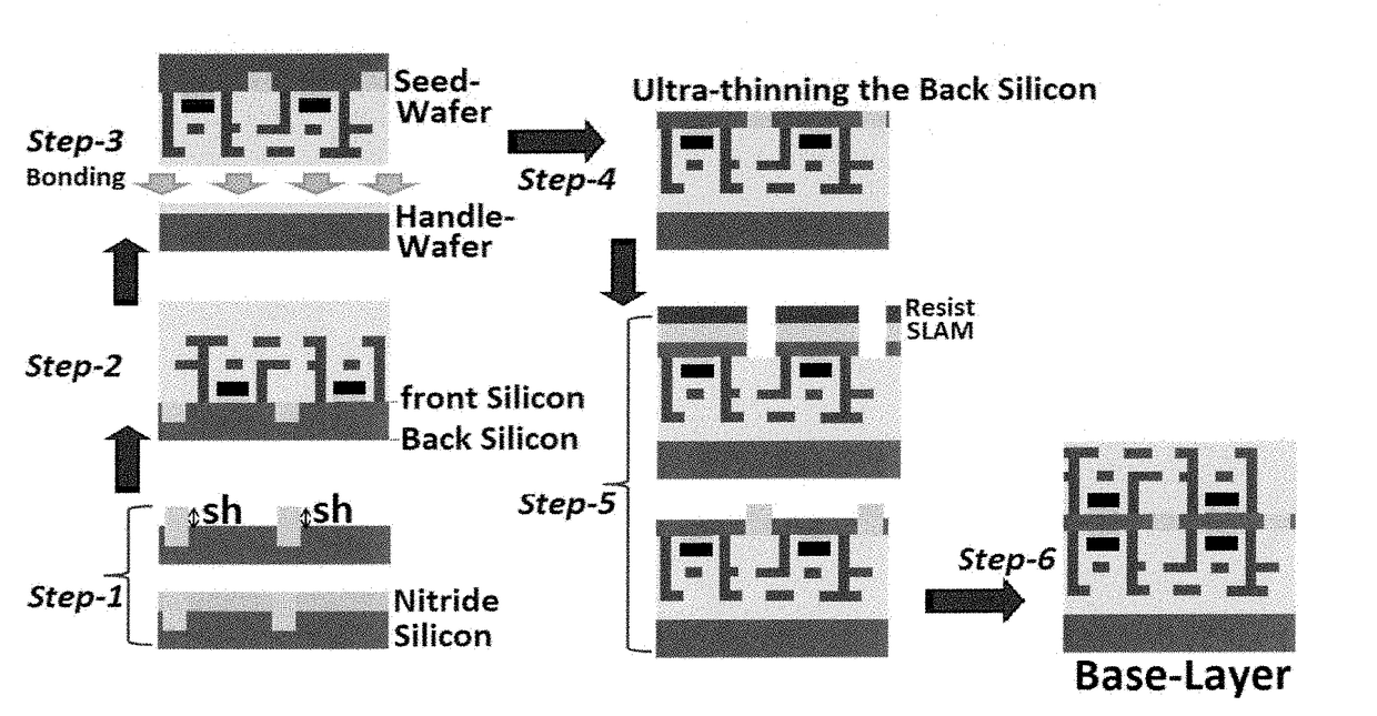
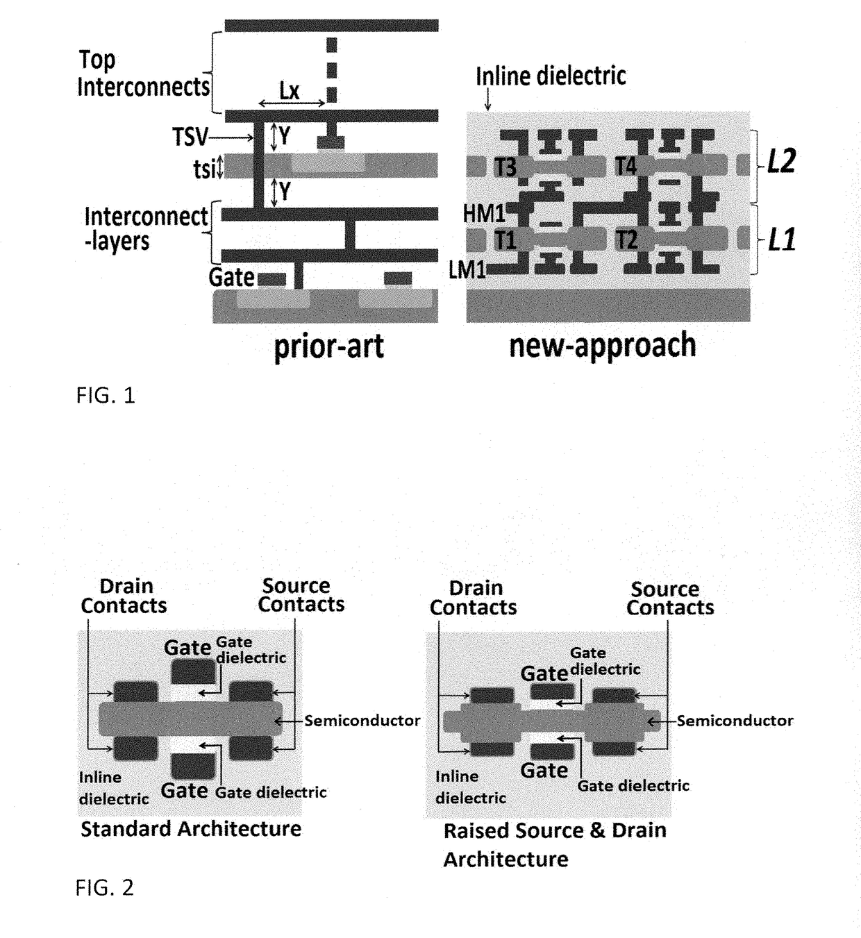
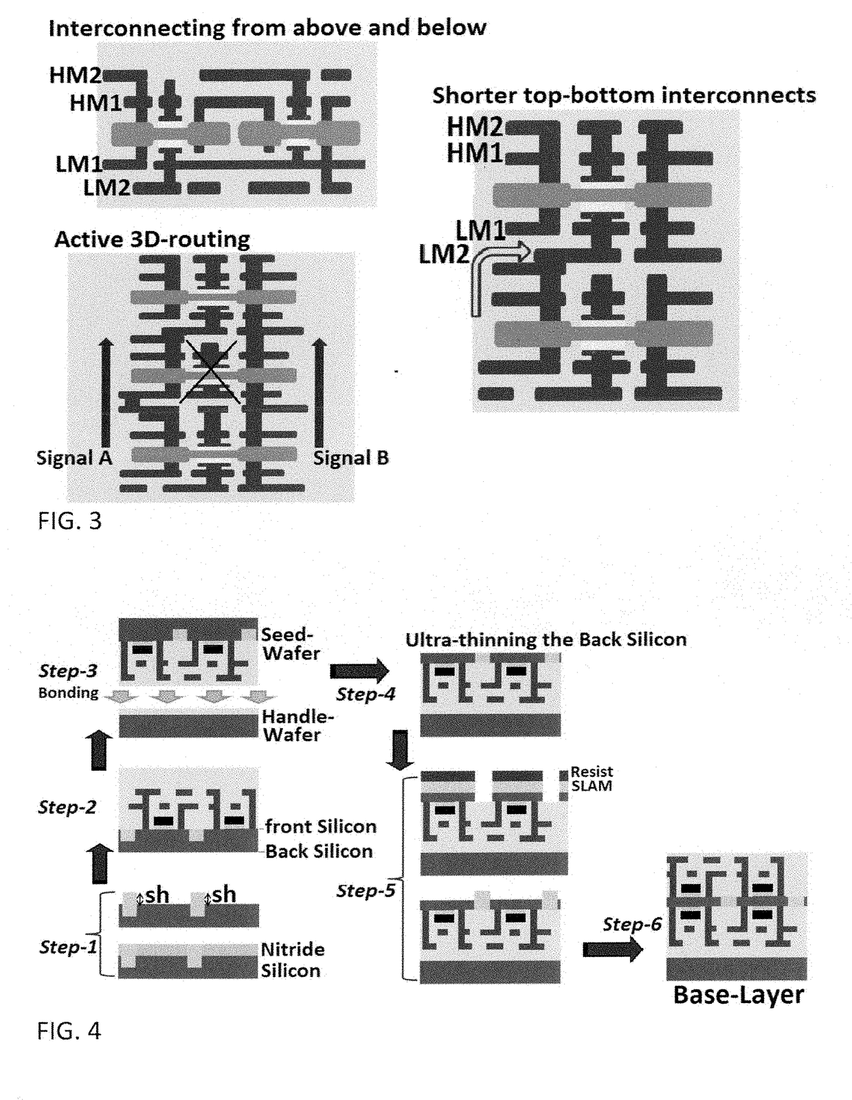
[0013]The approach can vertically integrate any number of Silicon layers with any number of high and low Inline interconnect-layers in each Silicon layer. The number of low Inline interconnect-layers in any Silicon layer can be different than the number of its high Inline interconnect-layers. Aside from the shorter top-to-bottom interconnects that this new-approach (of this patent) brings by enabling to directly connect the top Contact(s) of one device to the bottom Contact(s) of another, it has few additional advantages over all prior arts: 1) It allows more ease and flexibility to interconnect the transistors in same Silicon layer (or Silicon plane) by interconnecting these transistors from above and / or from below. This can further reduce the lengths, the RC-delays and the power consumed in interconnecting the devices (transistors) that are laid in same Silicon layer. 2) It enables active 3D-routing of electric signals with purposely switched On / Off devices. This enables reconfigu...


PUM


Abstract

Method to fabricate high-rise three-dimensional Integrated-Circuits (3D-ICs) is described. It has the major advantage over all the other known methods and prior arts to fabricate or manufacture 3D-ICs in that it substantially reduces RC-delays and fully eliminates or very substantially reduces the large and bulky electrically conductive Through-Silicon-VIAs in monolithic 3D integration. This enables the 3D-ICs to have faster operational speed with denser device integration.

Description

BACKGROUND OF THE INVENTION[0001]As the Semiconductor industry is entering the era that foresees the end of miniaturization of the Silicon transistor, engineers are already considering newer approaches to boost the device density, the efficiency and the performance of the logic and the memory Chips without necessitating the move to smaller transistors. Although Three-Dimensional (3D) circuits are nothing new given that Integrated-Circuits (ICs) are routinely packaged nowadays one on top another via wire-bonds or large copper pillars called Through-Silicon-VIAs (TSVs) that vertically connect the ICs together, the concept has still limitations. For one thing, these 3D-Packages are interconnecting the subsystems together and not their discrete components. This is consequently limiting the density of 3D interconnections, and the overall Chip performance. Further, even in substituting wire-bonds with TSVs the resulting effects from RC-delays and higher impedances between subsystems were ...

Claims


Application Information

Patent Timeline
11 Oct 2018
Publication
US20180294284A1
IPC
H01L27/12; H01L23/00
CPC
H01L27/1207; H01L24/29; H01L24/83; H01L2224/83895; H01L21/8226; H01L29/78648; H01L21/76802; H01L27/0207
Inventors
TARAKJI, AHMAD; CHAUDHARY, NIRMAL