
Capacitor structure and method of manufacturing the same

a capacitor and capacitor area technology, applied in the field of semiconductor devices, can solve the problem that the capacitance value cannot be increased in the horizontal direction, and the capacitance area almost cannot be increased, so as to increase the mechanical strength of the capacitor structure and increase the capacitance valu

Active Publication Date: 2018-12-13
WINBOND ELECTRONICS CORP
View PDF3 Cites 2 Cited by
  • Summary
  • Abstract
  • Description
  • Claims
  • Application Information

AI Technical Summary

Benefits of technology

The invention provides a capacitor structure with a reinforcing structure that increases its mechanical strength and prevents deformation or tipping. The top supporting layer has a high-k material that can also be used as a portion of the capacitor dielectric layer, increasing capacitor area and capacitance value. The method of manufacturing the capacitor structure does not require a photomask, simplifying the process and reducing manufacturing costs.

Problems solved by technology

However, the memory cells of a high-integrity dynamic random access memory are generally very closely arranged, and therefore capacitor area almost cannot be increased in the horizontal direction, and the height of the capacitor needs to be increased in the perpendicular direction to increase capacitor area and capacitance value.

Method used


Image

  • Capacitor structure and method of manufacturing the same
  • Capacitor structure and method of manufacturing the same
  • Capacitor structure and method of manufacturing the same

Examples


Embodiment Construction

[0016]The invention is more comprehensively described with reference to the figures of the present embodiments. However, the invention may also be implemented in various different forms, and is not limited to the embodiments in the present specification. The thicknesses of the layers and regions in the figures are enlarged for clarity. The same or similar reference numerals represent the same or similar devices and are not repeated in the following paragraphs.

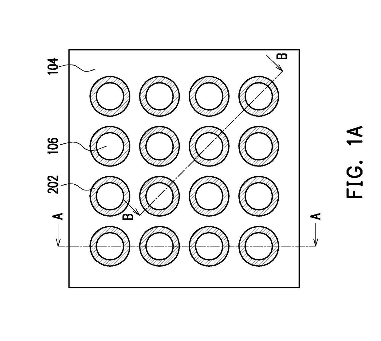
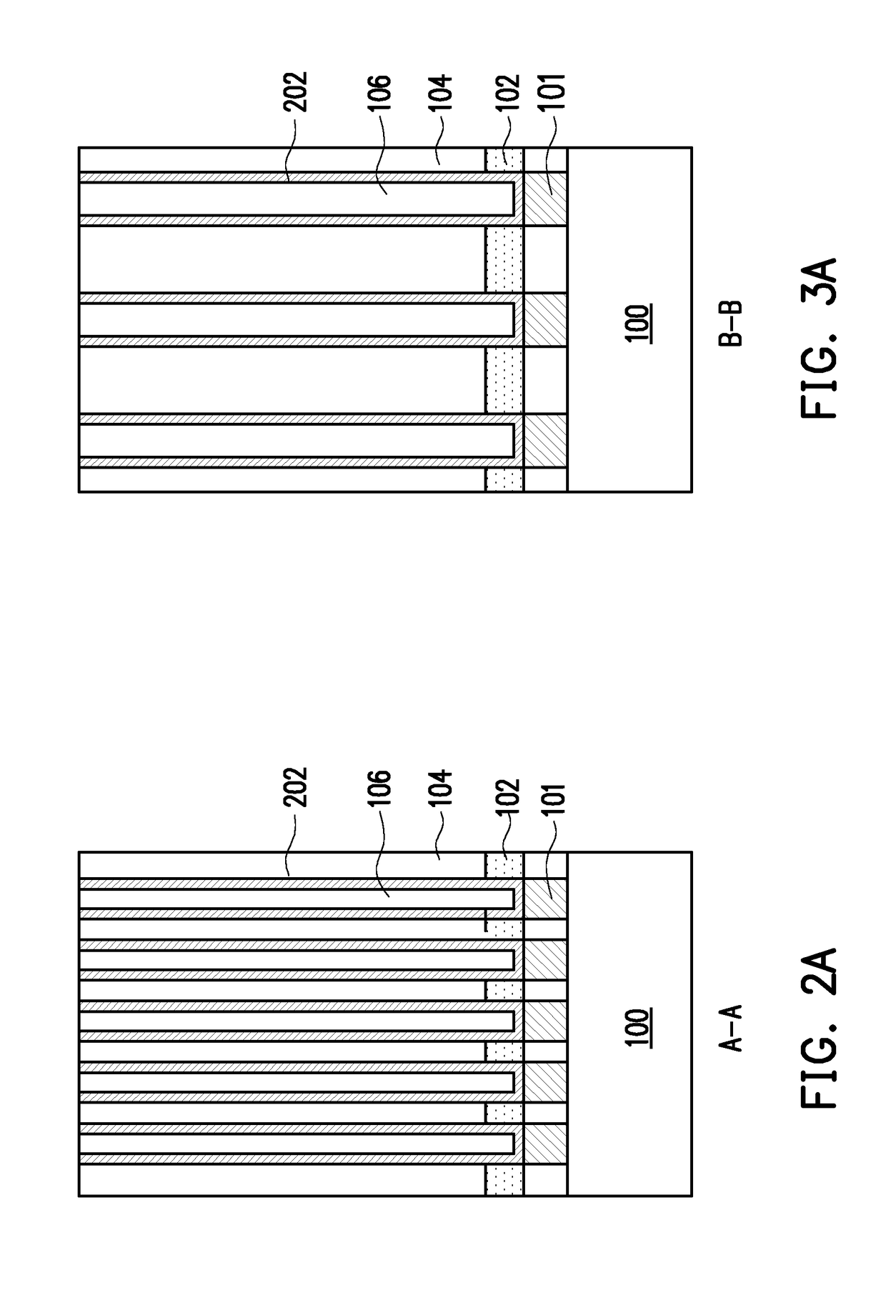
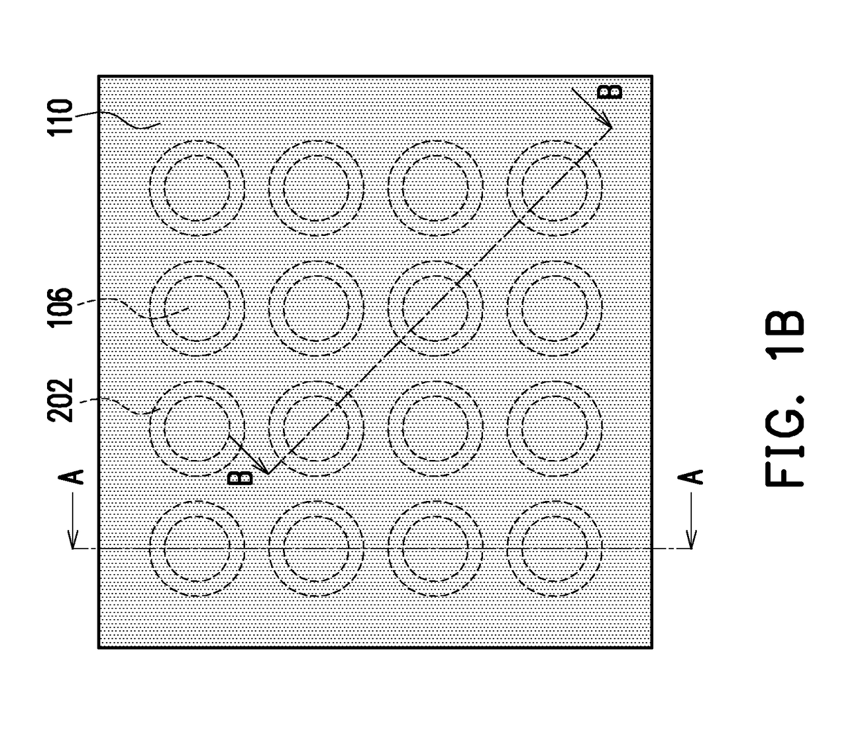
[0017]FIG. 1A to FIG. 1G are top views of a manufacturing process of a capacitor structure shown according to an embodiment of the invention. FIG. 2A to FIG. 2G are respectively cross sections along line A-A of FIG. 1A to FIG. 1G. FIG. 3A to FIG. 3G are respectively cross sections along line B-B of FIG. 1A to FIG. 1G.

[0018]Referring to all of FIG. 1A, FIG. 2A, and FIG. 3A, the present embodiment provides a method of manufacturing a capacitor structure including the following steps. First, a substrate 100 is provided. The substr...


PUM


Abstract

Provided is a capacitor structure including a substrate, a cup-shaped lower electrode, a top supporting layer, a capacitor dielectric layer, and an upper electrode. The cup-shaped lower electrode is located on the substrate. The top supporting layer surrounds the upper portion of the cup-shaped lower electrode. The top supporting layer includes a high-k material. Surfaces of the cup-shaped lower electrode and the top supporting layer are covered by the capacitor dielectric layer. A surface of the capacitor dielectric layer is covered by the upper electrode.

Description

CROSS-REFERENCE TO RELATED APPLICATION[0001]This application claims the priority benefit of China application serial no. 201710430909.4, filed on Jun. 9, 2017. The entirety of the above-mentioned patent application is hereby incorporated by reference herein and made a part of this specification.BACKGROUND OF THE INVENTIONField of the Invention[0002]The invention relates to a semiconductor structure and a method of manufacturing the same, and more particularly, to a capacitor structure and a method of manufacturing the same.Description of Related Art[0003]A dynamic random access memory is a volatile memory and is formed by a plurality of memory cells. Specifically, each memory cell is mainly formed by one transistor and one capacitor controlled by the transistor. The capacitor is mainly used to store charge representing data, and needs to have high capacitance to ensure data is not readily lost.[0004]With the progress of technology, every electronic product is being developed to have...

Claims


Application Information

Patent Timeline
Patent Type & Authority Applications(United States)
IPC IPC(8): H01L49/02H10N97/00
CPCH01L28/87H01L28/91H01L27/10805H01L28/40H10B12/30H10B12/033
Inventor PARK, CHEOL SOOCHEN, MING-TANGWANG, CHUN-CHIEH
Owner WINBOND ELECTRONICS CORP
Learn More