Power amplifier circuit

Active Publication Date: 2018-12-13
MURATA MFG CO LTD
View PDF1 Cites 8 Cited by
  • Summary
  • Abstract
  • Description
  • Claims
  • Application Information

AI Technical Summary

Benefits of technology

The invention aims to provide a power amplifier circuit that can prevent uneven temperature distribution among multiple transistors and maintain the circuit's performance.

Problems solved by technology

Hence, if, for example, a bipolar transistor is composed of a plurality of unit transistors, then the occurrence of temperature differences among the unit transistors causes a unit transistor having a relatively high temperature to undesirably draw in the collector currents of other unit transistors.
This may consequently lead to the occurrence of a phenomenon known as a current collapse phenomenon, in which the collector current of the entire transistor group composed of the plurality of unit transistors decreases.
However, if the resistance value of the emitter ballast resistor is excessively large, then the output power of the power amplifier circuit may decrease or power added efficiency may deteriorate.

Method used


Image

  • Power amplifier circuit
  • Power amplifier circuit
  • Power amplifier circuit

Examples


first embodiment

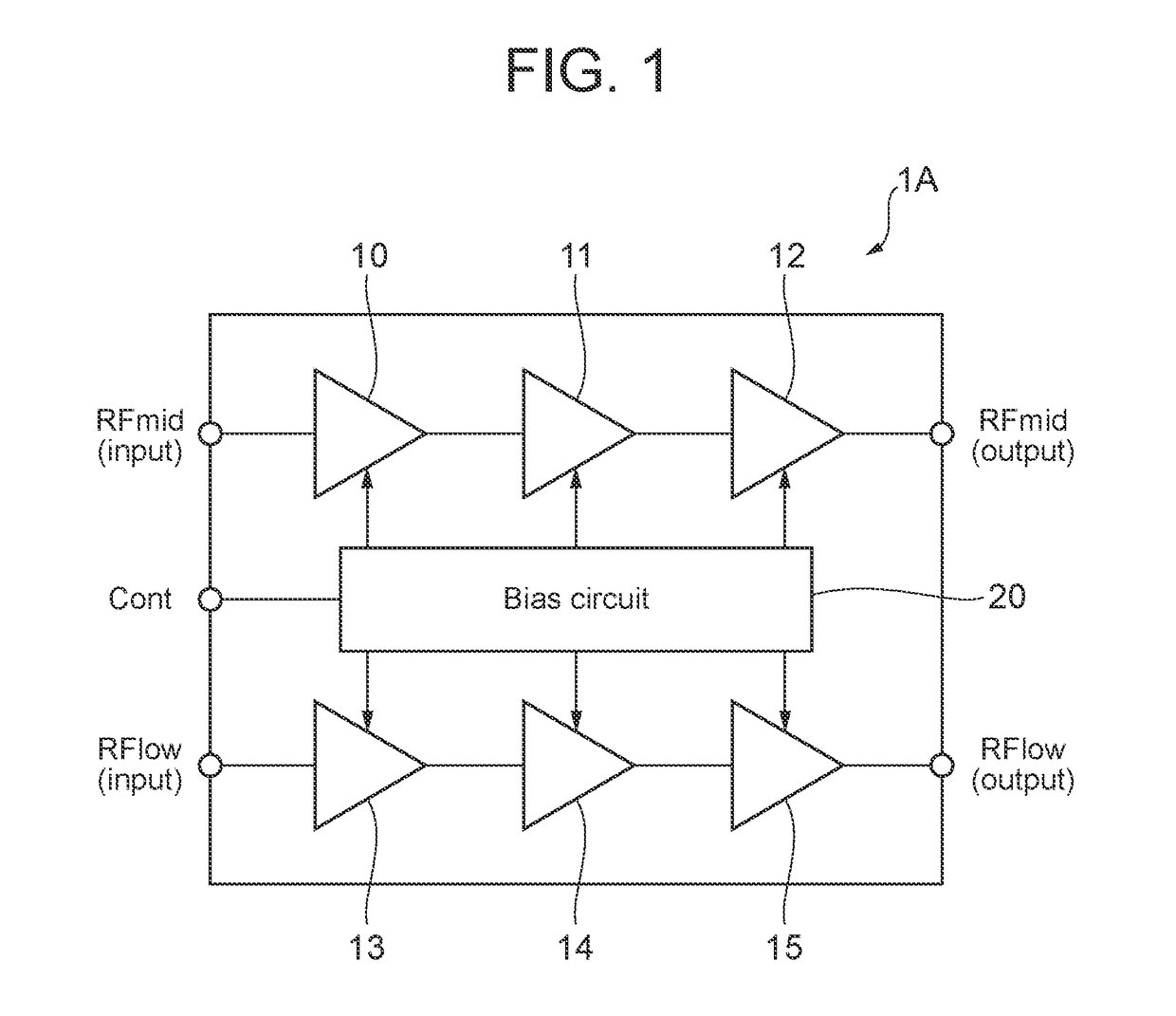
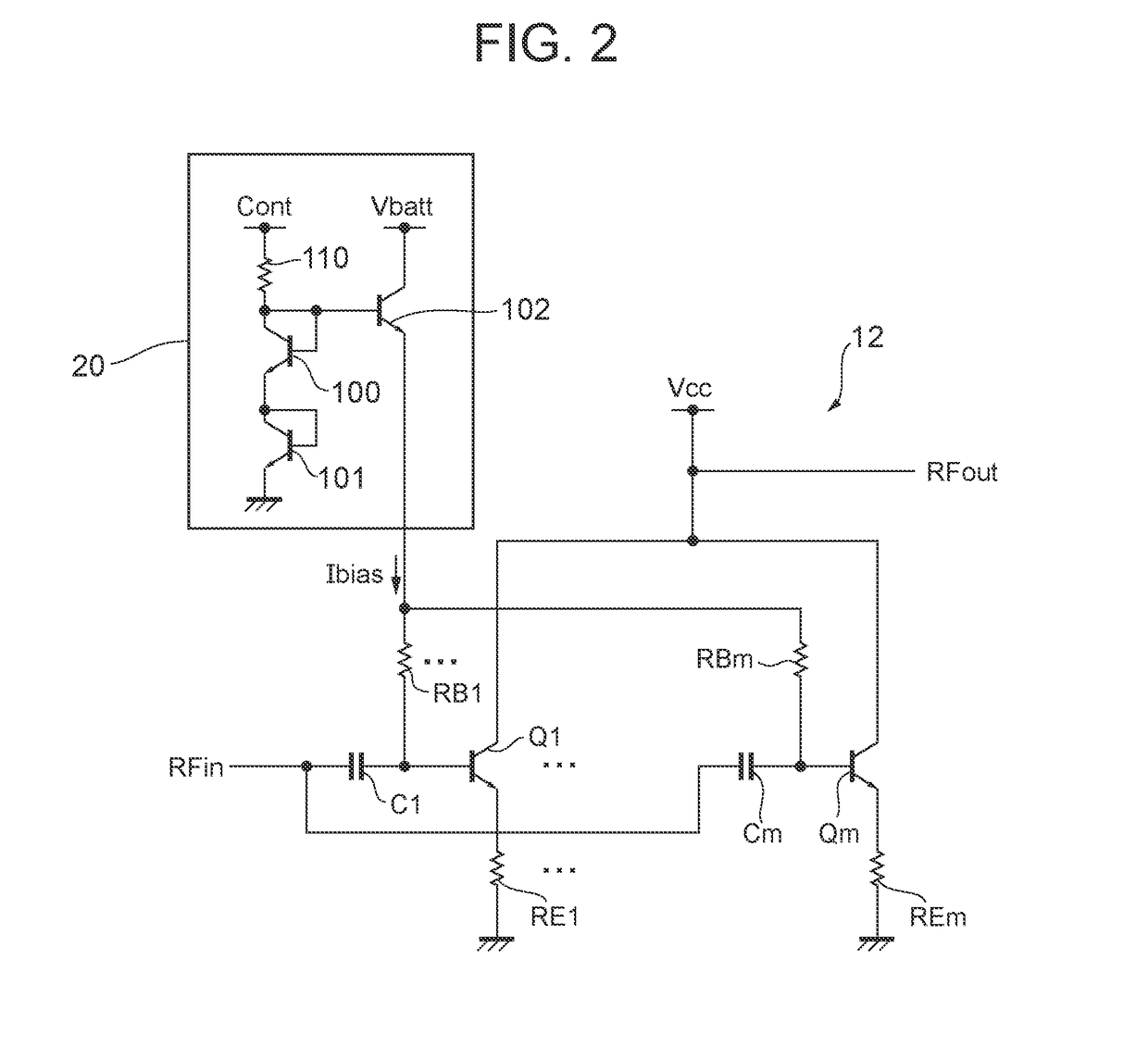
[0022]FIG. 1 is a diagram illustrating a configuration example of a power amplifier circuit according to the present invention. A power amplifier circuit 1A illustrated in FIG. 1 is, for example, installed in a cellular phone and used to amplify the power of radio frequency (RF) signals transmitted to a base station. The communication standards for the RF signals to be amplified include, for example, the second generation mobile communication system (2G), the third generation mobile communication system (3G), the fourth generation mobile communication system (4G), the fifth generation mobile communication system (5G), the long term evolution (LTE)-frequency division duplex (FDD), the LTE-time division duplex (TDD), the LTE-Advanced, and LTE-Advanced Pro. The communication standards for the signals to be amplified by the power amplifier circuit 1A are not limited to the above.

[0023]The power amplifier circuit 1A has, for example, two amplification paths. To be specific, the power amp...

second embodiment

[0045]FIG. 6 is a diagram illustrating a configuration example of a power amplifier circuit according to the present invention. A power amplifier circuit 1B illustrated in FIG. 6 differs from the power amplifier circuit 1A illustrated in FIG. 1 in that both the first path and the second path are provided with two systems of amplifiers in the third stage.

[0046]To be specific, the power amplifier circuit 1B has amplifiers 30 and 31 in place of the amplifier 12, and also has amplifiers 32 and 33 in place of the amplifier 15. The amplifier 30 and the amplifier 31, and the amplifier 32 and the amplifier 33 are appropriately used according to the operation mode of the power amplifier circuit 1B. More specifically, an example of the first path of a middle band will be described. For example, if the power amplifier circuit 1B is in a high power mode (a first mode) for outputting power of a predetermined level or more, then both the amplifiers 30 and 31 will be turned on, and if the power am...

third embodiment

[0051]FIG. 8 is a diagram illustrating an example of the circuit diagram of amplifiers and bias circuits included in a power amplifier circuit according to the present invention. A power amplifier circuit 1C illustrated in FIG. 8 differs from the power amplifier circuit 1B illustrated in FIG. 7 in that an amplifier 31 does not have the resistive elements RB1b to RBnb.

[0052]In other words, in the power amplifier circuit according to the present embodiment, it is not always necessary to provide all unit transistors with both the emitter ballast resistors and the base ballast resistors. As illustrated in FIG. 8, some transistors may be provided with the emitter ballast resistors and the base ballast resistors, whereas the other transistors may be provided with either the emitter ballast resistors or the base ballast resistors. For example, the power amplifier circuit 1C employs the configuration in which unit transistors Q1a to Qma (i.e., the unit transistors that operate only in the h...


PUM


Abstract

A power amplifier circuit is capable of restraining uneven temperature distribution among a plurality of unit transistors while restraining the deterioration of the characteristics of the power amplifier circuit. The power amplifier circuit includes: a first transistor group which includes a plurality of unit transistors and which amplifies an input signal and outputs an amplified signal; a bias circuit which supplies a bias current or a bias voltage to a base or a gate of each unit transistor of the first transistor group; a plurality of first resistive elements, each of which is connected between the base or the gate of each unit transistor of the first transistor group and an output of the bias circuit; and a plurality of second resistive elements, each of which is connected between an emitter or a source of each unit transistor of the first transistor group and a reference potential.

Description

[0001]This application claims priority to U.S. Provisional Application Ser. No. 62 / 516,811, filed on Jun. 8, 2017, entitled “POWER AMPLIFIER”, the entirety of which is incorporated herein by reference.BACKGROUNDField[0002]The present invention relates to a power amplifier circuit.Description of Related Art[0003]A power amplifier circuit mounted in mobile communication equipment, such as a cellular phone, usually uses a bipolar transistor as an amplifier. The bipolar transistor has a thermal positive feedback characteristic, in which, as the temperature of a transistor device increases, a collector current increases, causing the temperature to further rise with a resultant increase in the collector current. Hence, if, for example, a bipolar transistor is composed of a plurality of unit transistors, then the occurrence of temperature differences among the unit transistors causes a unit transistor having a relatively high temperature to undesirably draw in the collector currents of oth...

Claims


Application Information

Patent Timeline
IPC IPC(8): H03F1/30H03F1/02H03F3/21H03F3/19H01L29/73H01L29/737
CPCH03F1/302H03F1/0205H03F3/21H03F3/19H01L29/7304H01L29/7371H03F2200/451H03F2200/447H03F2200/21H03F3/211H03F3/4508H03F2203/45031H01L29/41708H01L27/0772H03F1/0277H03F1/30H03F3/195H03F3/72H03F2200/408
Inventor MATSUI, TOSHIKISASAKI, KENJIHARIMA, FUMIO
Owner MURATA MFG CO LTD
Why Eureka
Try Eureka