

Chemical mechanical polishing slurry composition and method of fabricating semiconductor device using the same
a technology of chemical mechanical polishing and slurry composition, which is applied in the direction of electrical equipment, chemistry apparatus and processes, other chemical processes, etc., can solve the problems of adversely affecting the yield and reliability of the semiconductor device, dishing and scratching, etc., and achieves the effect of improving dishing and scratching, and high oxide film-to-semiconductor film polishing selectivity
Inactive Publication Date: 2018-12-20
SAMSUNG ELECTRONICS CO LTD +1
View PDF3 Cites 3 Cited by
- Summary
- Abstract
- Description
- Claims
- Application Information
AI Technical Summary
Benefits of technology
The present invention provides a chemical mechanical polishing (CMP) slurry composition that has a high selectivity for oxide films and semiconductor films, and can improve dishing and scratching. Additionally, the invention provides a method of fabricating a semiconductor device that improves reliability and yield.
Problems solved by technology
It may be difficult for a CMP slurry composition having a relatively high selectivity and a relatively high removal rate to control flatness in an area having small steps, and the CMP slurry composition may cause dishing and scratching.
Such problems may cause various defects in a semiconductor device manufactured using the CMP process which may adversely affect the yield and reliability of the semiconductor device.
Method used
View moreImage
Smart ImageViewing Examples

Examples
example 1
[0049]A CMP slurry composition was prepared by mixing 5% by weight of ceria having a particle size of 100 nm as abrasive particles, 0.1% by weight of arginine as a first cationic compound, 0.07% by weight of acetic acid as a second cationic compound, and 0.01% by weight of 4,7,10-trioxamidecane-l 13-diamine (TTD) as a nonionic compound.
example 2
[0064]A CMP slurry composition was prepared in the same manner as in Example 1, except that the content of the nonionic compound was changed to 0.03% by weight.
Login to View More PUM
| Property | Measurement | Unit |
|---|---|---|
| size | aaaaa | aaaaa |
| size | aaaaa | aaaaa |
| size | aaaaa | aaaaa |
Abstract
Provided are a chemical mechanical polishing (CMP) slurry composition and a method of fabricating a semiconductor device using the same. The chemical mechanical polishing (CMP) slurry composition includes abrasive particles, a first cationic compound which comprises at least any one of an amino acid, a polyalkylene glycol, a polymer polysaccharide to which a glucosamine compound is bonded, and a polymer containing an amine group, a second cationic compound which comprises an organic acid, and a nonionic compound which comprises polyetheramine.
Description
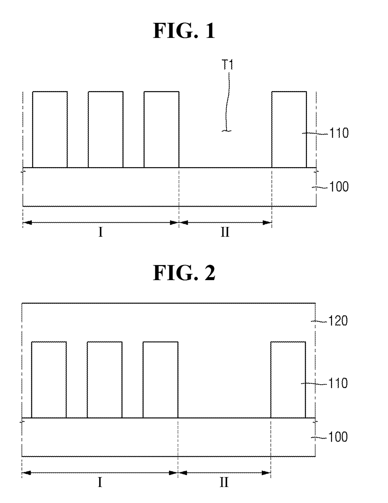
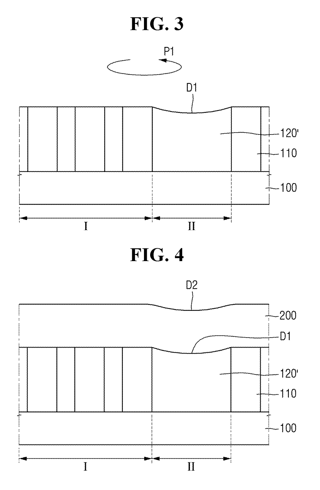
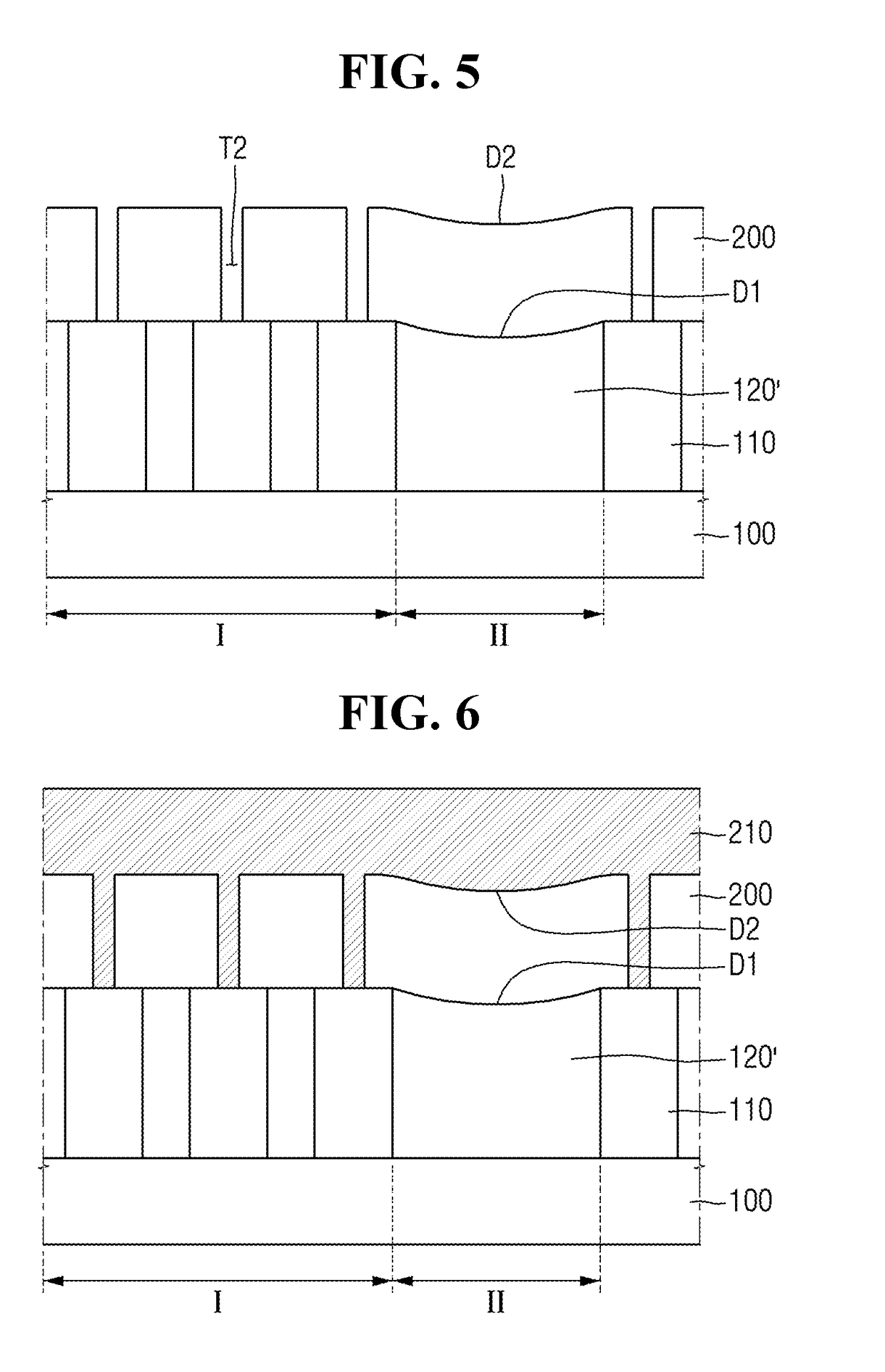
[0001]This application claims the benefit of Korean Patent Application No. 10-2017-0076462, filed on Jun. 16, 2017, in the Korean Intellectual Property Office, the disclosure of which is incorporated herein in its entirety by reference.BACKGROUND1. Technical Field[0002]The present disclosure relates to a chemical mechanical polishing (CMP) slurry composition and a method of fabricating a semiconductor device using the same, and more particularly, to a CMP slurry composition including a polishing control agent and a method of fabricating a semiconductor device using the CMP slurry composition.2. Description of the Related Art[0003]As a film planarization process, an etch-back process, a reflow process, a chemical mechanical polishing (CMP) process, or the like can be used. The CMP process is widely used for wide-area planarization and highly integrated circuits because it is advantageous for wide-area planarization and has excellent flatness.[0004]In the CMP process, an object to be ...
Claims
Login to View More Application Information
Patent Timeline
 Patent Type & AuthorityApplications(United States)
IPC IPC(8): C09G1/02H01L21/3105
CPCC09G1/02H01L21/31055H01L21/31051H01L21/31053C09K3/1454H01L21/30625H01L21/3212
InventorPARK, SEUNG HOKWON, CHANG GILLEE, SUNG PYOHWANG, JUN HAKIM, SANG KYUNPARK, HYE SUNGSHIN, SU YOUNGLEE, WOO INLEE, YANG HEEPARK, JONG HYUKYOON, IL YOUNG
OwnerSAMSUNG ELECTRONICS CO LTD