

Cerium oxide powder, method for preparing the same, and CMP slurry comprising the same
a technology of silicon oxide and slurry, which is applied in the direction of lanthanide oxide/hydroxide, other chemical processes, cellulosic plastic layered products, etc., can solve the problems of low polishing selectivity of the insulating silicon oxide layer to the silicon nitride layer, drop in the margin, and degradation of the quality of a transistor or device, so as to improve the polishing selectivity of the silicon oxide layer and the effect of increasing the polishing ra
- Summary
- Abstract
- Description
- Claims
- Application Information
AI Technical Summary
Benefits of technology
Problems solved by technology
Method used
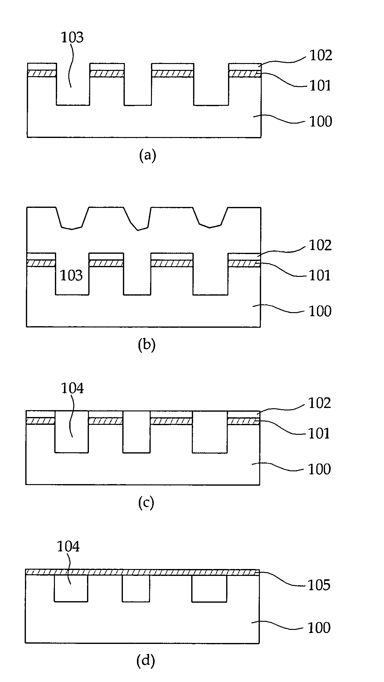
Image

Examples
example 1
Preparation of Cerium Oxide Powder
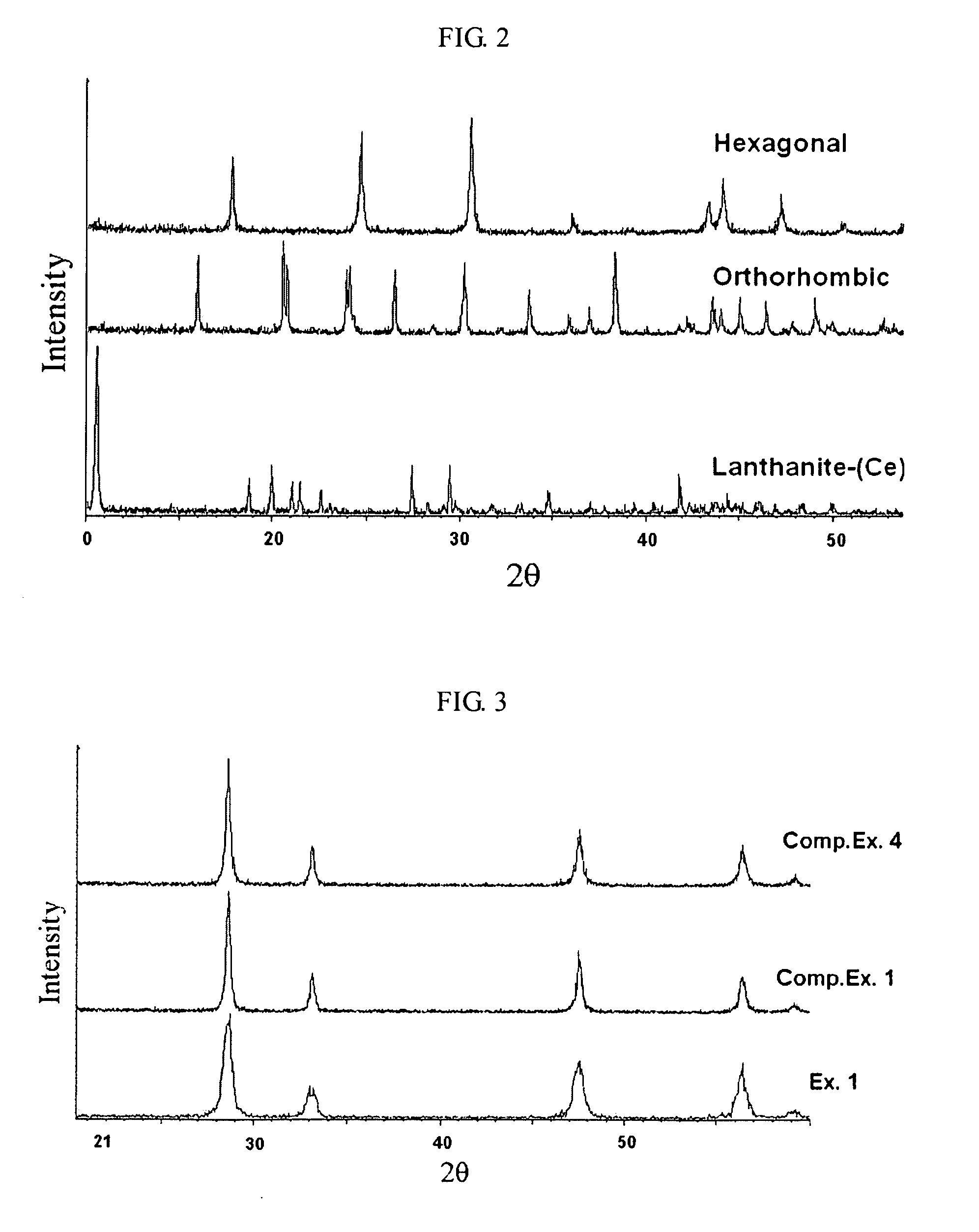
[0084]First, 1 kg of cerium carbonate powder having a hexagonal crystal structure (see XRD data in FIG. 2) was charged into an alumina crucible, was calcined at 350° C. for 12 hours under oxidative atmosphere to which air is fed sufficiently, and was crushed by using a jet mill. The crushed powder is further calcined at 750° C. for 2 hours to obtain light yellow-colored cerium oxide powder.
[0085]After analyzing the powder by XRD, it can be seen that a complete phase transition from cerium carbonate into cerium oxide is accomplished, as shown in FIG. 3.
[0086]Photographs of the cerium carbonate powder and the cerium oxide powder taken by SEM are shown in FIG. 4 and FIG. 5, respectively.
Preparation of CMP Slurry
[0087]A cerium oxide dispersion was prepared by using 0.5 kg of the cerium oxide powder obtained as described above, 25 g of a dispersant (polyacrylic acid available from Aldrich) and 5 L of pure water. The cerium oxide dispersion was titrated t...
example 2
[0091]Cerium oxide powder and CMP slurry comprising the same were provided in the same manner as described in Example 1, except that the second calcination step was carried out at 850° C. for 2 hours. The cerium oxide powder dispersed in the CMP slurry had an average particle diameter of 176 nm and a particle size distribution of 70˜300 nm.
example 3
[0092]Cerium oxide powder and CMP slurry comprising the same were provided in the same manner as described in Example 1, except that the second calcination step was carried out at 950° C. for 2 hours. The cerium oxide powder dispersed in the CMP slurry had an average particle diameter of 182 nm and a particle size distribution of 70˜300 nm.
PUM
| Property | Measurement | Unit |
|---|---|---|
| particle diameter | aaaaa | aaaaa |
| temperature | aaaaa | aaaaa |
| temperature | aaaaa | aaaaa |
Abstract
Description
Claims
Application Information