Electroabsorption optical modulator

a technology of optical modulator and optical modulator, which is applied in the field of electroabsorption optical modulator, can solve the problems of limited use of such devices, low optical modulation efficiency of most such devices that have been studied to date, and limited speed of optical modulation operation, so as to reduce light absorption, improve modulation efficiency, and high-efficiency optical coupling

Inactive Publication Date: 2018-12-27
NEC CORP +1
View PDF0 Cites 11 Cited by
  • Summary
  • Abstract
  • Description
  • Claims
  • Application Information

AI Technical Summary

Benefits of technology

[0015]It is an object of the present invention to provide an electroabsorption optical modulator capable of realizing highly efficient optical coupling with a Si waveguide, improving modulation efficiency, reducing light absorption by an electrode layer and achieving low optical loss.
[0019]According to one aspect of the present invention, it is possible to provide an electroabsorption optical modulator using GeSi capable of realizing highly efficient optical coupling with a Si waveguide, improving modulation efficiency, reducing light absorption by an electrode layer and achieving low optical loss.

Problems solved by technology

However, optical switches and optical modulators that use a thermo-optic effect of silicon to change the refractive index operate at low speed, and accordingly their use is limited to cases of device speeds corresponding to modulation frequencies not higher than 1 Mb / second.
Most of such devices that have been studied to date have low optical modulation efficiency, and accordingly, for optical phase modulation, require a length on the order of millimeters and an injection current density higher than 1 kA / cm3.
If the device size is large, the device becomes susceptible to the influence of temperature distribution over the silicon platform, and it is therefore assumed that a change in the refractive index of the silicon layer caused by a thermo-optic effect due to the temperature distribution cancels out the essentially existing electro-optic effect, thus raising a problem.
However, the speed of the optical modulation operation is limited by the lifetime of free carriers in rib 1 and carrier diffusion in rib 1 when the forward bias is removed.
However, there is the problem that the introduced impurities lower the optical modulation efficiency.
While, theoretically, high speed operation of the PN junction could be achieved by applying a reverse bias, it requires a relatively high drive voltage or a large device size.
However, in practice there is a problem in that the region where the carrier density dynamically changes is an extremely thin region with a size of about several tens of nanometers, which results in the problem that an optical modulation length on the order of millimeters is required, and the electro-optic modulator accordingly becomes large in size, and consequently high speed operation is difficult.
It is a problem with the electroabsorption optical modulator using GeSi disclosed in Non-patent Literature 2 how to efficiently optically couple with a Si waveguide, improve modulation efficiency, reduce light absorption by the electrode layer and achieve low optical loss.
It is another problem with the electroabsorption optical modulator that the operation wavelength band is narrow and the operation wavelength band varies along with a temperature variation.
Although this GeSi electroabsorption optical modulator is enabled to operate at high speed, the electrode layer is formed by stacking a GeSi layer on the Si waveguide and subjecting the GeSi layer to p-type or n-type doping, which results in a problem that the optical coupling length increases and light absorption loss by the p- or n-doped GeSi electrode layer is large.

Method used


Image

  • Electroabsorption optical modulator
  • Electroabsorption optical modulator
  • Electroabsorption optical modulator

Examples


Embodiment Construction

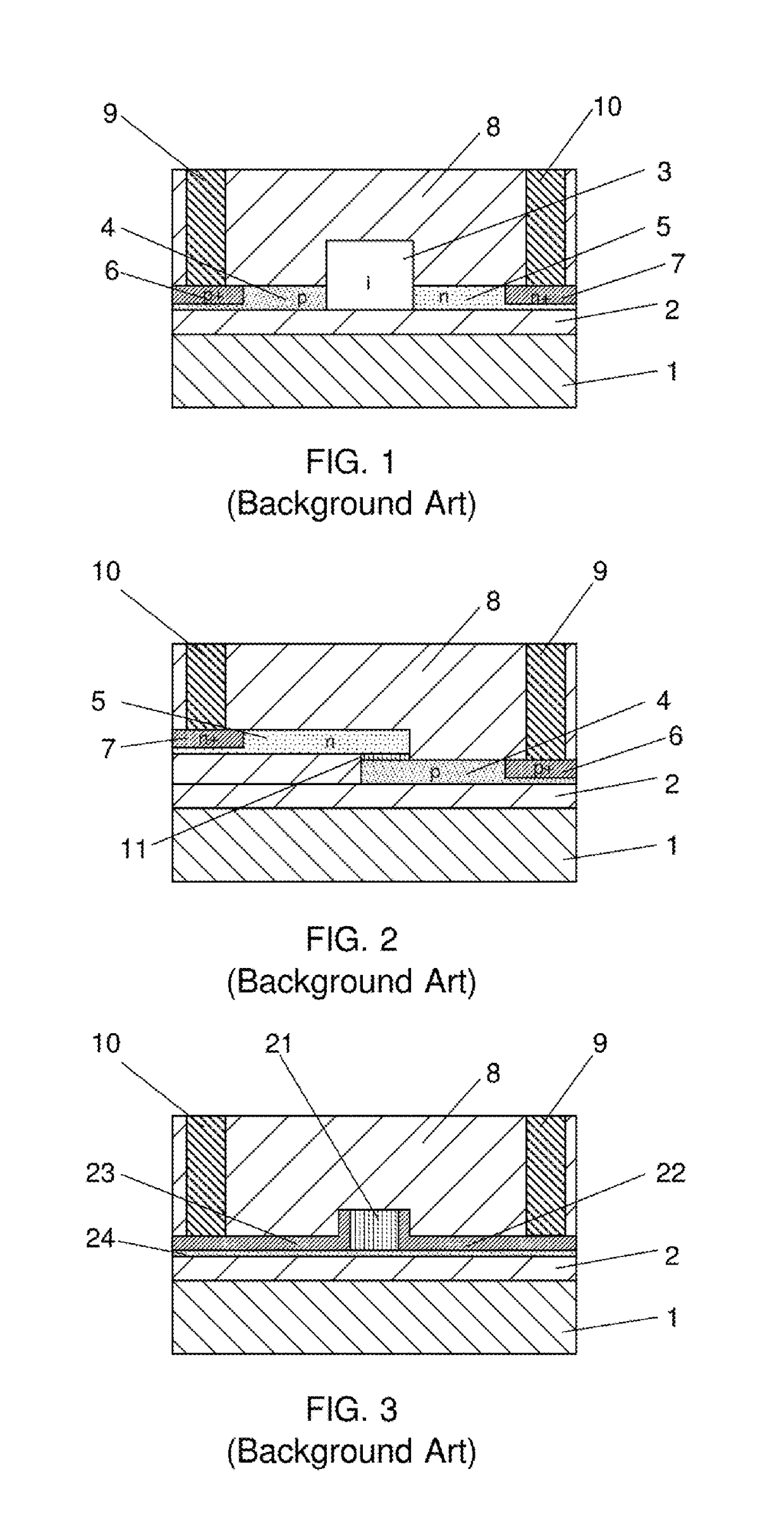
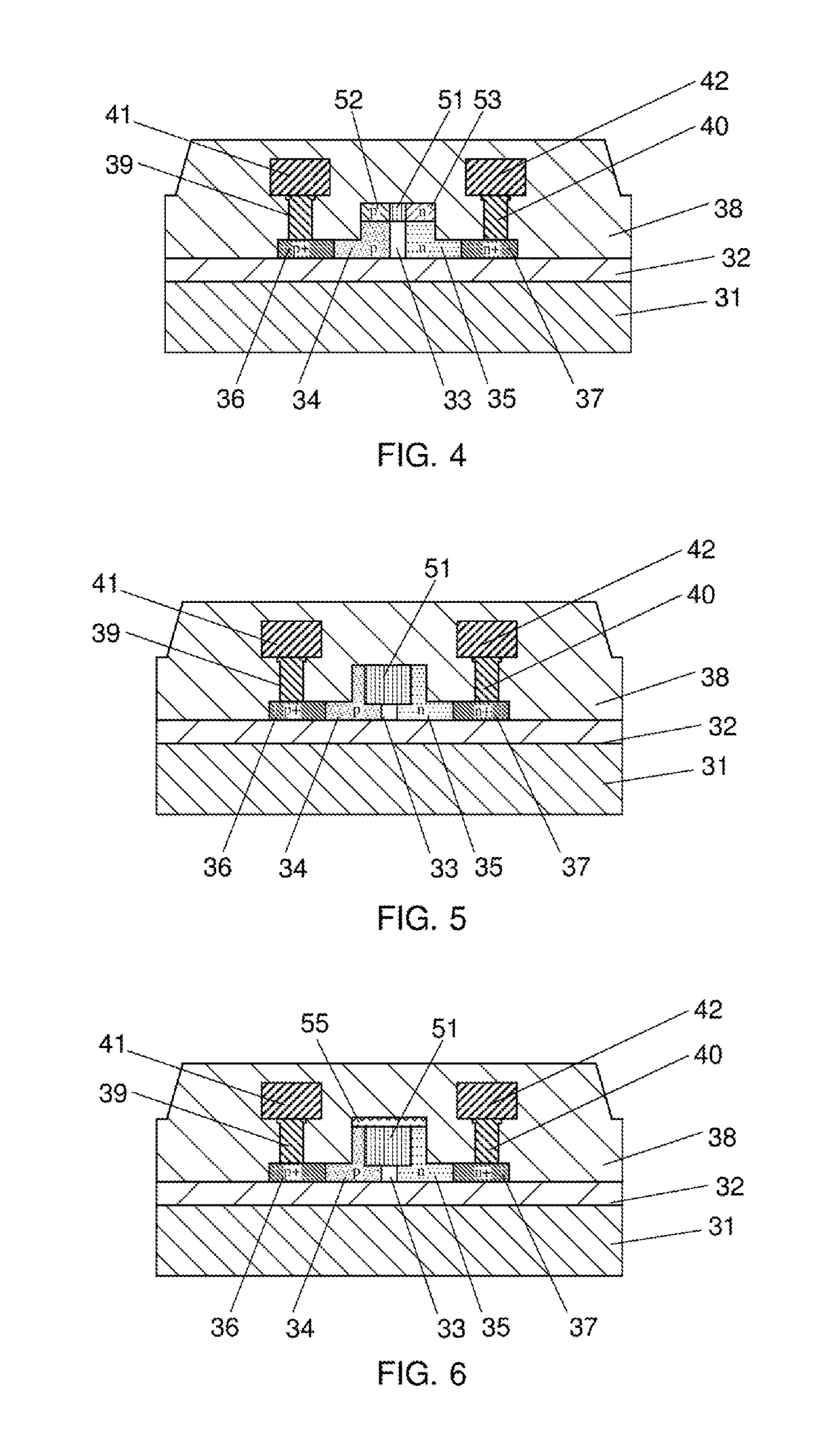
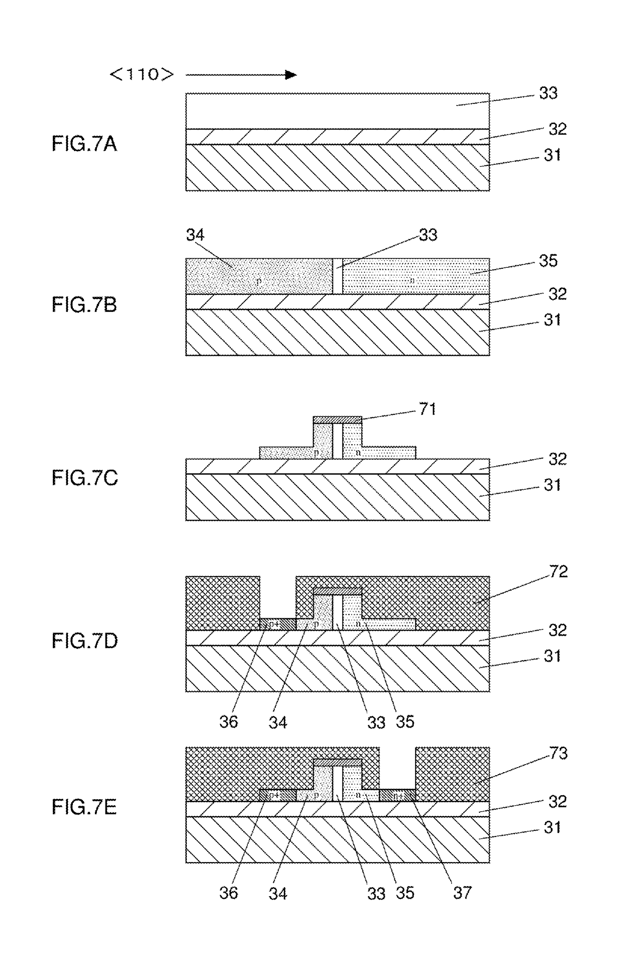
[0029]Hereinafter, the present invention will be described with example embodiments.

[0030]In an electro-optic modulator (electroabsorption optical modulator) according to the present example embodiment, as shown in FIG. 4, by forming first silicon (Si) layer 34 doped so as to exhibit a first type of conductivity (for example, p-type conductivity) and second silicon (Si) layer 35 doped so as to exhibit a second type of conductivity (for example, n-type conductivity), both being disposed parallel to support substrate 31 of an SOI substrate via buried oxide (BOX) layer 32 which constitutes a lower clad, stacking germanium-silicon (GeSi) layer 51 on the doped first and second Si layers, further subjecting the GeSi layer to p-type and n-type doping to form electrode layers 52 and 53, it is possible to reduce light absorption by the electrode layers. Note that support substrate 31 and BOX layer 32 may be simply collectively called a “substrate.”

[0031]In this case, third Si layer 33 made u...


PUM

PropertyMeasurementUnit
communication wavelengthsaaaaaaaaaa
carrier densityaaaaaaaaaa

Abstract

An electroabsorption optical modulator capable of realizing optical coupling with a Si waveguide with high efficiency, improving modulation efficiency, reducing light absorption by an electrode layer and achieving low optical loss includes first Si layer 34 of a first conductive type and second Si layer 35 of a second conductive type disposed parallel to substrate 31 and GeSi layer 51 stacked on the first and second Si layers.

Description

INCORPORATION BY REFERENCE[0001]This application is based upon and claims the benefit of priority from Japanese patent application No. 2017-124291, filed on Jun. 26, 2017, the disclosure of which is incorporated herein in its entirety by reference.TECHNICAL FIELD[0002]The present invention relates to an electroabsorption optical modulator according to an electro-optic effect for high speed conversion of high speed electrical signals into optical signals that is required in the information processing and telecommunications fields.BACKGROUND ART[0003]Silicon-based optical communication devices functioning at 1310 and 1550 nm fiber-optic communication wavelengths for a variety of systems such as for fiber-to-the-home and local area networks (LANs) are highly promising technologies which enable integration of optical functioning elements and electronic circuits together on a silicon platform by means of CMOS technologies.[0004]In recent years, silicon-based passive optical devices such ...

Claims


Application Information

Patent Timeline
Patent Type & Authority Applications(United States)
IPC IPC(8): G02F1/025
CPCG02F1/025G02F2001/0157G02F2202/10G02F2201/063G02F1/0157
Inventor FUJIKATA, JUNICHI
Owner NEC CORP
Why Eureka
Try Eureka