Check patentability & draft patents in minutes with Patsnap Eureka AI!

Chemical vapor phase growth apparatus

Inactive Publication Date: 2019-01-03
NATIONAL CHIAO TUNG UNIVERSITY
View PDF5 Cites 0 Cited by
  • Summary
  • Abstract
  • Description
  • Claims
  • Application Information

AI Technical Summary

Benefits of technology

The present invention is a chemical vapor phase growth apparatus that includes a plurality of sub-reaction chambers with upper heating elements set at different temperatures. This apparatus can solve the problem of impurities in precursors by adjusting the upper heating elements to the thermal cracking temperatures of the precursors in the same sub-reaction chamber. This minimizes impurities from entering the films, resulting in high-quality film materials. Additionally, the apparatus can grow high-quality films at low temperatures and reduce gas-phase side reactions. It also has a better chance to accomplish atomic layer deposition for a given film, especially a multi-element compound. Overall, this apparatus provides a more efficient and effective method for film fabrication.

Problems solved by technology

However, too high or too low temperature also impairs the film deposition.
Since this will bring about the generation of large quantities of structure, point defects and / or the decomposition of the deposited film.
It is obviously that the sole substrate temperature to meet all the demands is not an easy job.
rnary. For these material growths, the CVD reactor equipped with only substrate heater is apparently unable to meet all the cracking demands of the source precursors, not to mention the need for the surface chemical rea
ctions. This inevitably leads to a narrowed growth window and often fails to attain the best film quality for these ma
Nevertheless, the abovementioned CVD systems respectively have different limitations in use.
The basic limitations thereof are the limitation in available precursors and the limitation in the types of films grown.
The limitations of the CWCVD system are due to the facts that the sole heating element thereof has to provide the substrate temperature for growing the film but also the thermal energy for cracking the precursors either homogeneously or heterogeneously.
On the contrary, if the cracking temperatures of the source precursors are too high and the grown film is highly thermally unstable, increasing the substrate temperature though can improve the cracking efficiency of source precursor, it often causes the decomposition / sublimation of the film itself, leading to the generation of large amounts of vacancies and defects, disfavoring the fabrication of high-quality materials.
Since if it does occur, it will generate non-negligible amounts of nanometer- or micrometer-scale particles in the vapor phase, causing considerably the depletion of source precursors.
Moreover, when these particles are incorporated into the solid, they certainly deteriorate seriously the film quality.
However, such a CVD system is not always being applicable for multi-element film growths.
This is because the more the source precursors used, the higher the chance of side reactions takes place.
Once the side reactions arise either by single source itself or by the gas-phase interactions among several precursors, they will inevitably provoke chained reactions, and cause the losses of source precursors, disfavoring the growth of the film.
Nevertheless, the ALE growth of multi-element compound by MSCVD system is a tough job to be implemented.
This sole substrate temperature has to fulfill the demands of the pyrolysis of all the source precursors into their proper active species and concurrently to satisfy the demands of the self-limiting growth conditions of individual binaries in multi-element compound, making such atomic layer growth truly difficult.
For these reasons, it is generally accepted that the conventional MSCVD technology is not yet fully ready for the preparation of the atom layer growth of multi-element compounds, especially with high material quality.

Method used


Image

  • Chemical vapor phase growth apparatus
  • Chemical vapor phase growth apparatus
  • Chemical vapor phase growth apparatus

Examples


Embodiment Construction

[0027]The following embodiments are used to further demonstrate the characteristics of the chemical vapor phase growth apparatus of the present invention. However, the films mentioned in the embodiments are only for conveniently explaining the present invention but not for limiting the scope of the present invention.

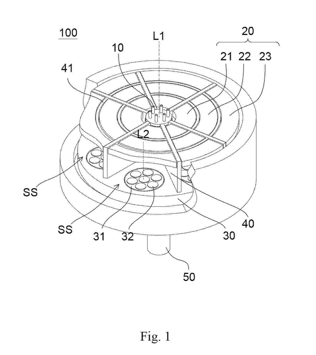
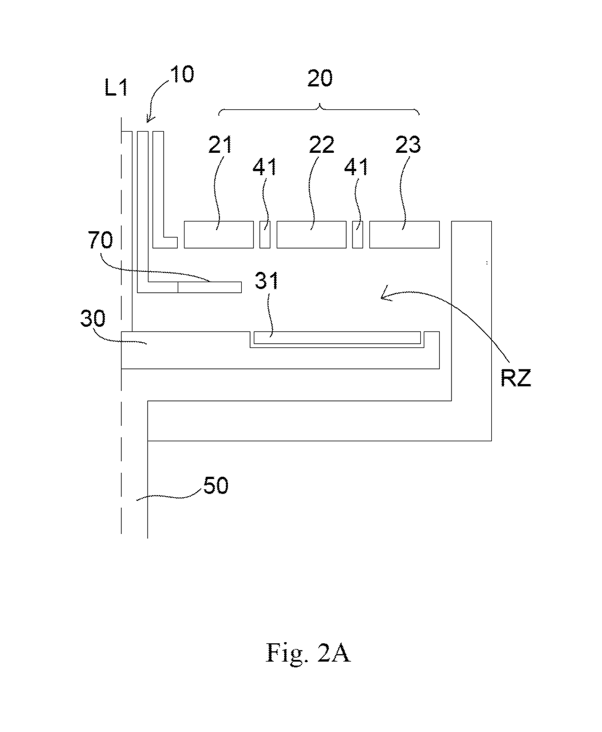
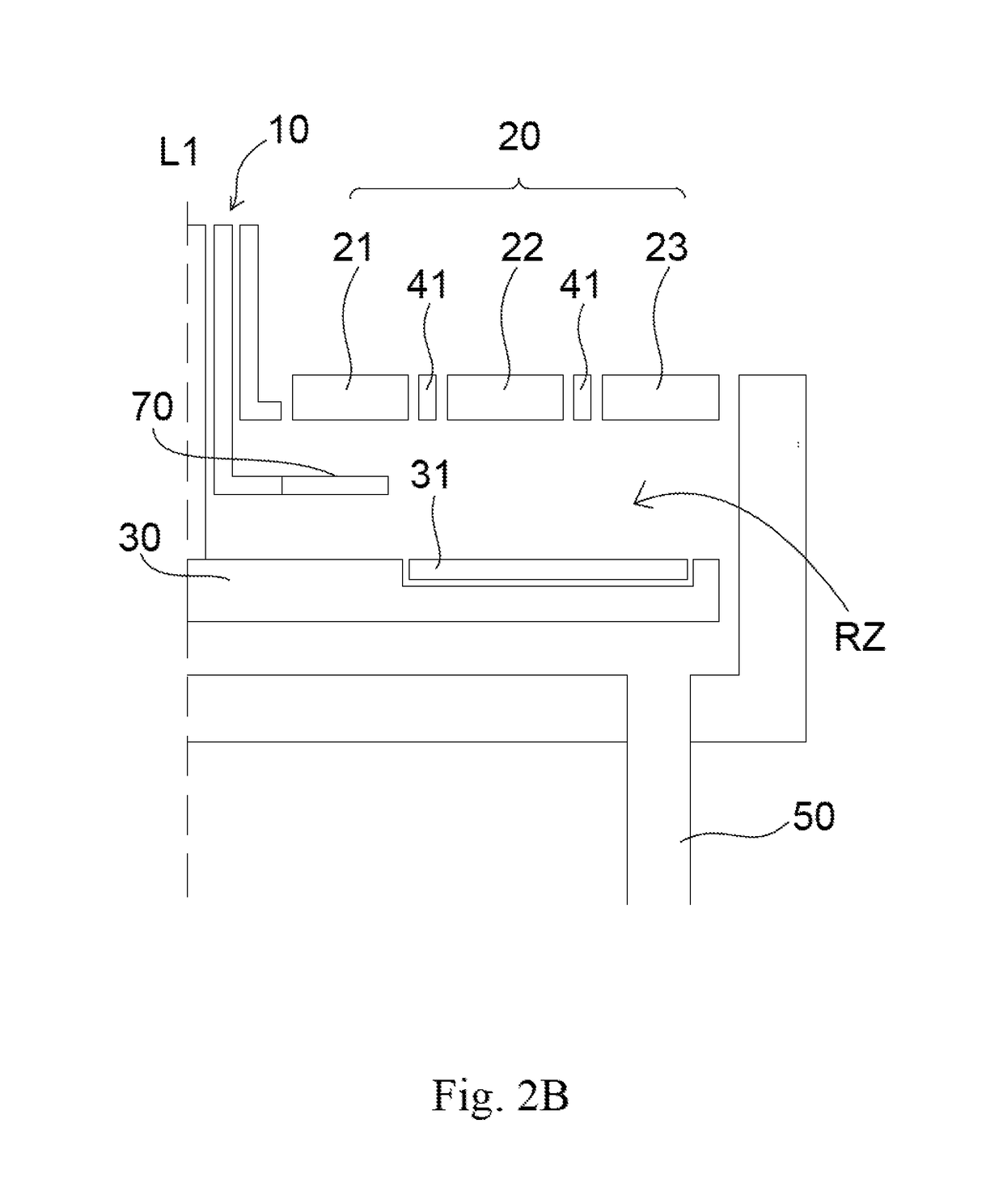
[0028]Referring to FIG. 1, the chemical vapor phase growth apparatus 100 of the present invention comprises of a lower heating element 30, wherein a plurality of carrier disks 31 is arranged on the lower heating element 30, and wherein each carrier disk 31 carries a plurality of substrates 32 where films are deposited; a plurality of partitions 40 is arranged at positions above the lower heating element to divide the reaction chamber into a plurality of sub-reaction chambers SS. Each sub-reaction chamber SS further comprises an upper heating element 20 made up of a plurality of thermostated upper heating units 21, 22 and 23 separated by insulators 41. The upper heating e...


PUM

PropertyMeasurementUnit
Angleaaaaaaaaaa
Flow rateaaaaaaaaaa
Frequencyaaaaaaaaaa

Abstract

A chemical vapor phase growth apparatus for growing films on substrates comprises of a thermostated lower heating element, including a plurality of carrier disks thereon, wherein each carrier disk further includes a plurality of substrates thereon for film deposition; a plurality of partitions, disposed above the lower heating element to define a plurality of sub-reaction chambers; a plurality of upper heating elements made of a plurality of thermostated upper heating units, disposed over the lower heating element by a gap to form reaction zones in each sub-reaction chamber; a gas inlet installed in each sub-reaction chamber to provide at least one precursor into the sub-reaction chamber; and a gas outlet installed in the chemical vapor phase growth apparatus to exhaust the gases.

Description

BACKGROUND OF THE INVENTION1. Field of the Invention[0001]The present invention relates to a chemical vapor phase growth apparatus, particularly a chemical vapor phase growth apparatus having a plurality of sub-reaction chambers with upper heating elements and a shared lower heating element, wherein the upper heating element of each sub-reaction chamber including a plurality of thermostated upper heating units is arranged in the upper region of the sub-reaction chamber. The lower heating element is to provide the substrate temperature for film growth and the upper heating element in each sub-reaction chamber together with the lower heating element is to form a 3D (both radial and the vertical directions) temperature profile in each individual sub-reaction chamber.2. Description of the Prior Art[0002]Chemical vapor deposition (CVD) apparatus is commonly used to fabricate different types of materials, such as insulators, conductors and semiconductors. The CVD apparatus has been used t...

Claims


Application Information

Patent Timeline
IPC IPC(8): C23C16/46
CPCC23C16/463C23C16/44C23C16/45544C23C16/24C23C16/303C23C16/403C23C16/4412C23C16/45551C23C16/4584C23C16/46
Inventor CHEN, WEI-KUOCHENG, CHUN-HUNG
Owner NATIONAL CHIAO TUNG UNIVERSITY
Features
  • R&D
  • Intellectual Property
  • Life Sciences
  • Materials
  • Tech Scout
  • Unparalleled Data Quality
  • Higher Quality Content
  • 60% Fewer Hallucinations
Learn More