

Photodetector focal plane array systems and methods based on microcomponents with arbitrary shapes
- Summary
- Abstract
- Description
- Claims
- Application Information
AI Technical Summary
Benefits of technology
Problems solved by technology
Method used
Image

Examples
Embodiment Construction
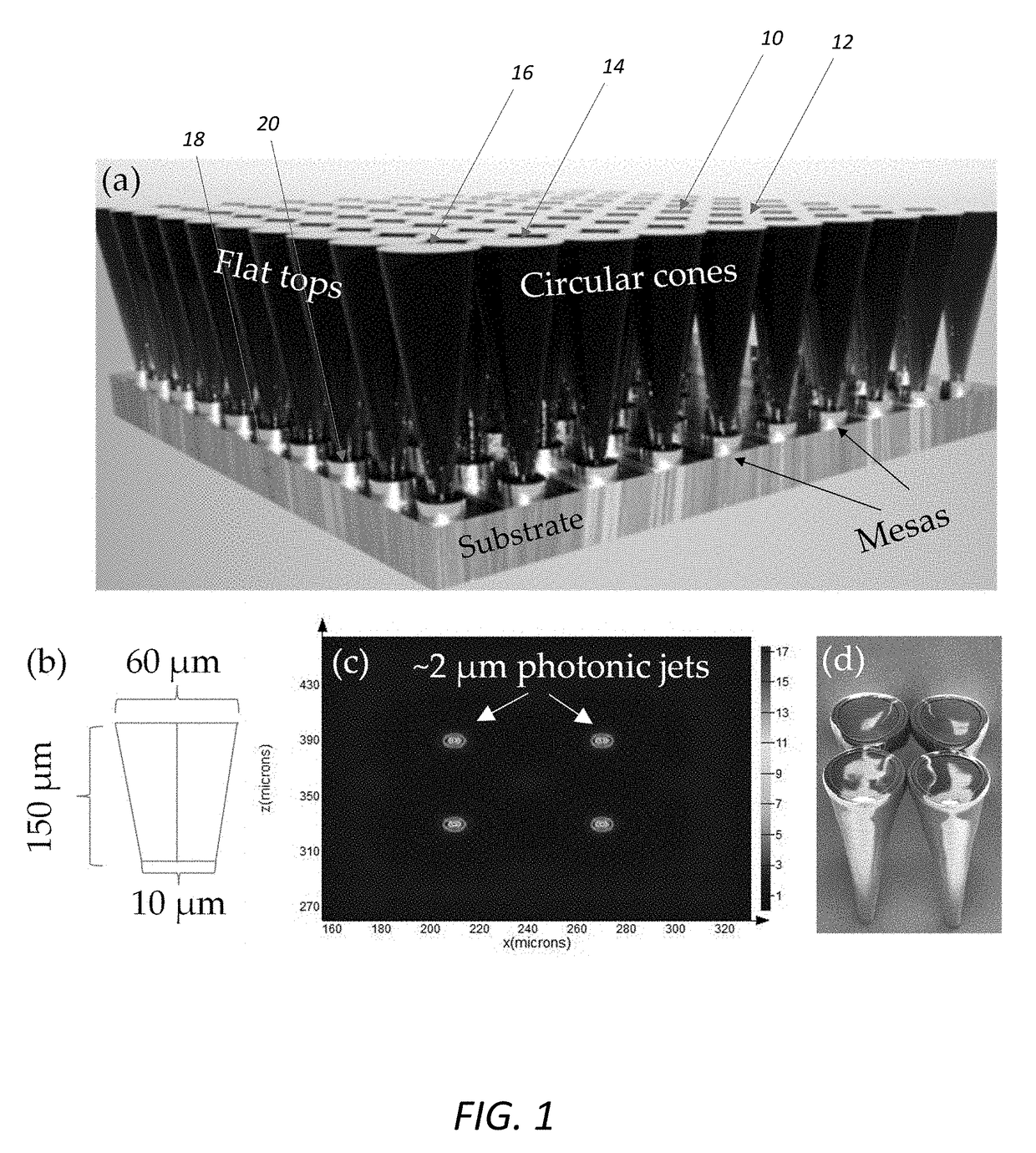
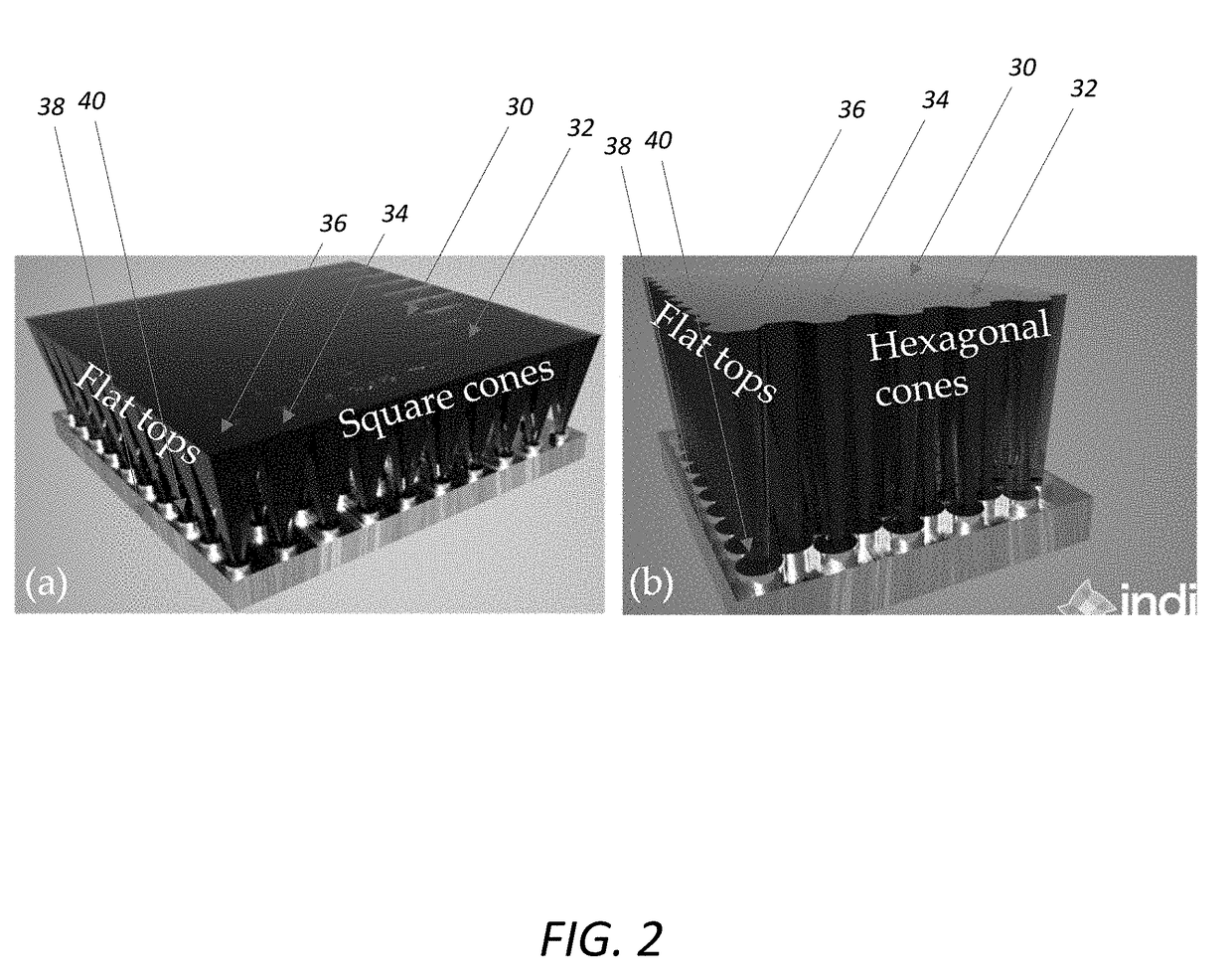
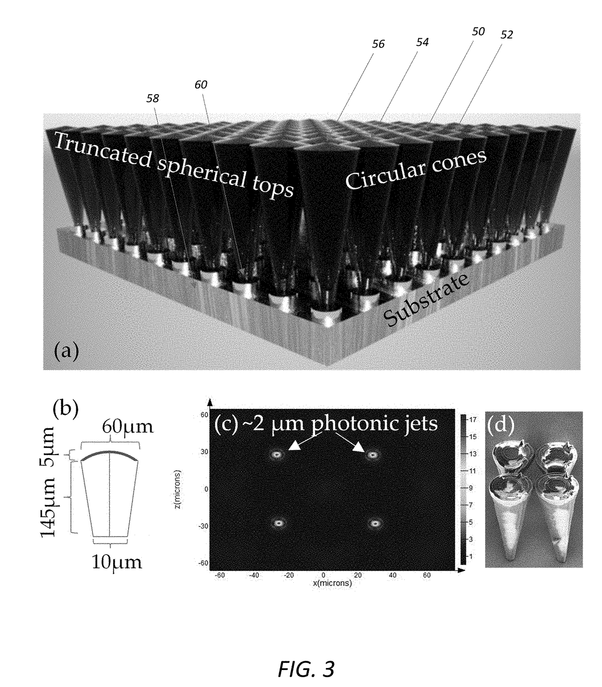
[0027]The present disclosure is based on the idea that, instead of using microspheres, one can use microcomponents with arbitrary shapes for enhancing the sensitivity and increasing the AOV of FPAs and the like. Although the focusing capability of such microcomponents has been established theoretically, the idea of their integration with FPAs has never been proposed or even expressed in previous studies.
[0028]The key to understanding this sensitivity enhancement is the fact that each of the microcomponents has an ability to collect light from an area that is much larger than the size of the associated photodetector mesa. The microcomponent is designed to operate as a focusing element and a waveguide, either in parallel or in series. As a result, each microcomponent couples light collected from an area that is significantly larger than the individual photodetector mesa into the given mesa. In U.S. Pat. No. 9,362,324 (Astratov et al.) microcomponents with circular symmetry, such as mi...
PUM
 Abstract
Description
Claims
Application Information