
Integrated Ultra-Compact VSWR Insensitive Coupler

a technology of ultra-compact and insensitive couplers, applied in the field ofcoupler circuits, to achieve the effect of reducing the areal size of the coupler

Active Publication Date: 2019-01-17
PSEMI CORP
View PDF2 Cites 3 Cited by
  • Summary
  • Abstract
  • Description
  • Claims
  • Application Information

AI Technical Summary

Benefits of technology

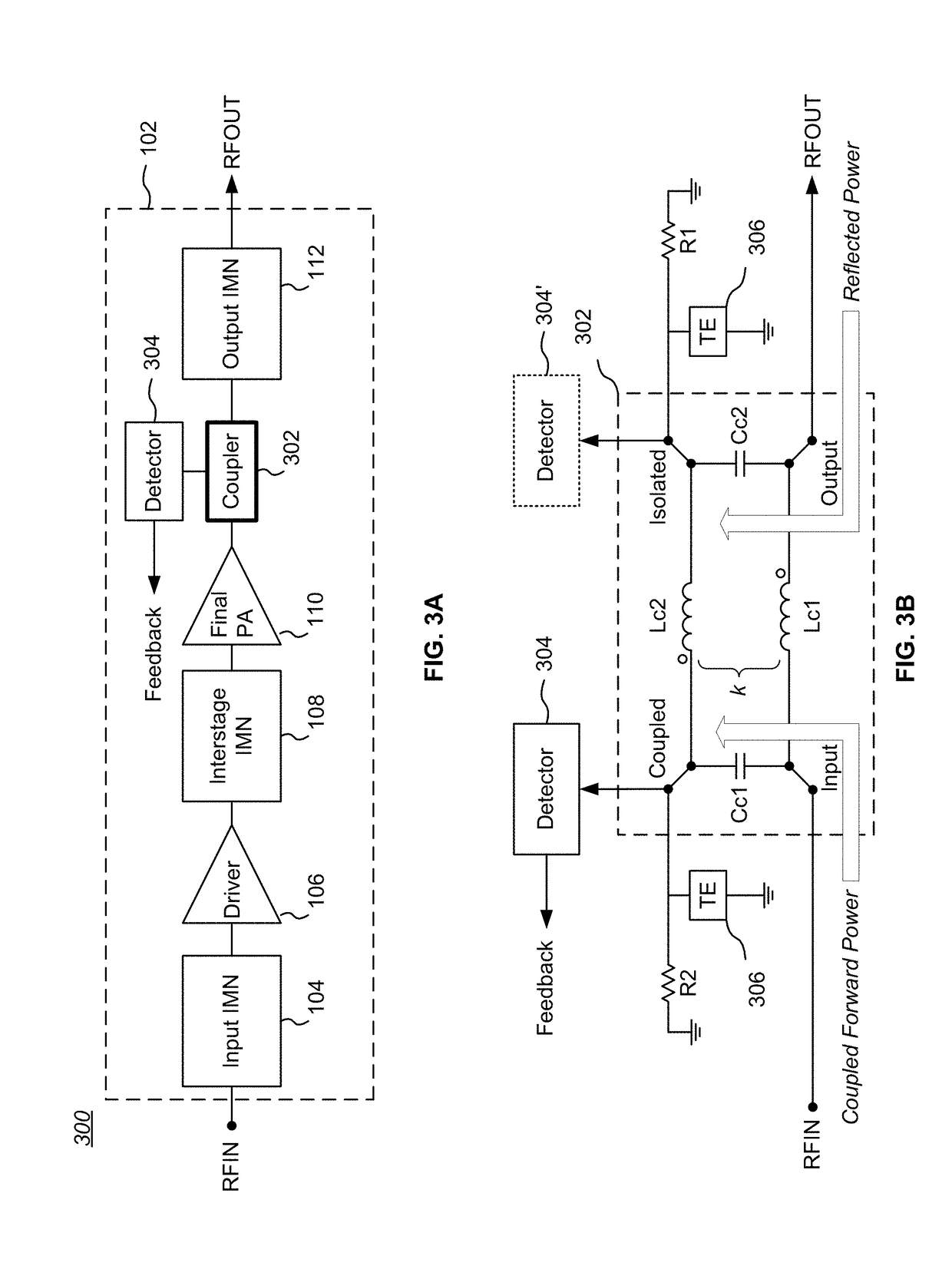
The patent text describes two embodiments where a coupler is placed between the final amplifier stage of a power amplifier and an output impedance matching network. The coupler is designed to operate in a low resistance environment and has a detector circuit, which results in a smaller size of the coupler. In the second embodiment, the coupler is integrated within the output impedance matching network, which further decreases the size of the coupler.

Problems solved by technology

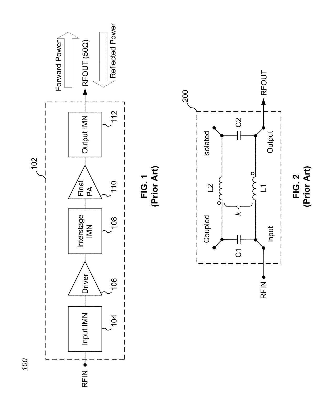
A problem with that solution is that reflected power, such as from an antenna, is also coupled into the power detector, causing the power detector to exhibit a sensitivity to the voltage standing wave ratio (VSWR) that exists at the output of the final amplifier stage 110 (VSWR is essentially the ratio of “reflected power” to “forward power”).

Method used


Image

  • Integrated Ultra-Compact VSWR Insensitive Coupler
  • Integrated Ultra-Compact VSWR Insensitive Coupler
  • Integrated Ultra-Compact VSWR Insensitive Coupler

Examples


performance examples

[0057]FIG. 6 is a graph of measured power Pout (in dB) versus phase angle (in degrees) measured at a detector circuit 304 capacitively coupled to RFOUT after the output impedance matching network 112 of an RF transmitter power amplifier 100. With a VSWR ratio of 3:1, power at the detector circuit 304 varies by about 8 dB.

[0058]In contrast, FIG. 7 is a graph of measured power Pout (in dB) versus phase angle (in degrees) measured at a detector circuit 304 connected to the Coupled port of a coupler 502 integrated within the output impedance matching network 504 of an RF transmitter power amplifier 508, as in FIG. 5C. Again using a VSWR ratio of 3:1 (and noting the significant difference in vertical scales between FIG. 6 and FIG. 7), power at the detector circuit 304 varies only by about 0.6 dB-about 7.5% of the power variation of the example shown in FIG. 6.

Feedback Example

[0059]Referring again to FIG. 5C, in operation, the transmitter 506 outputs modulated RF power (RFIN or Pin) to th...


PUM


Abstract

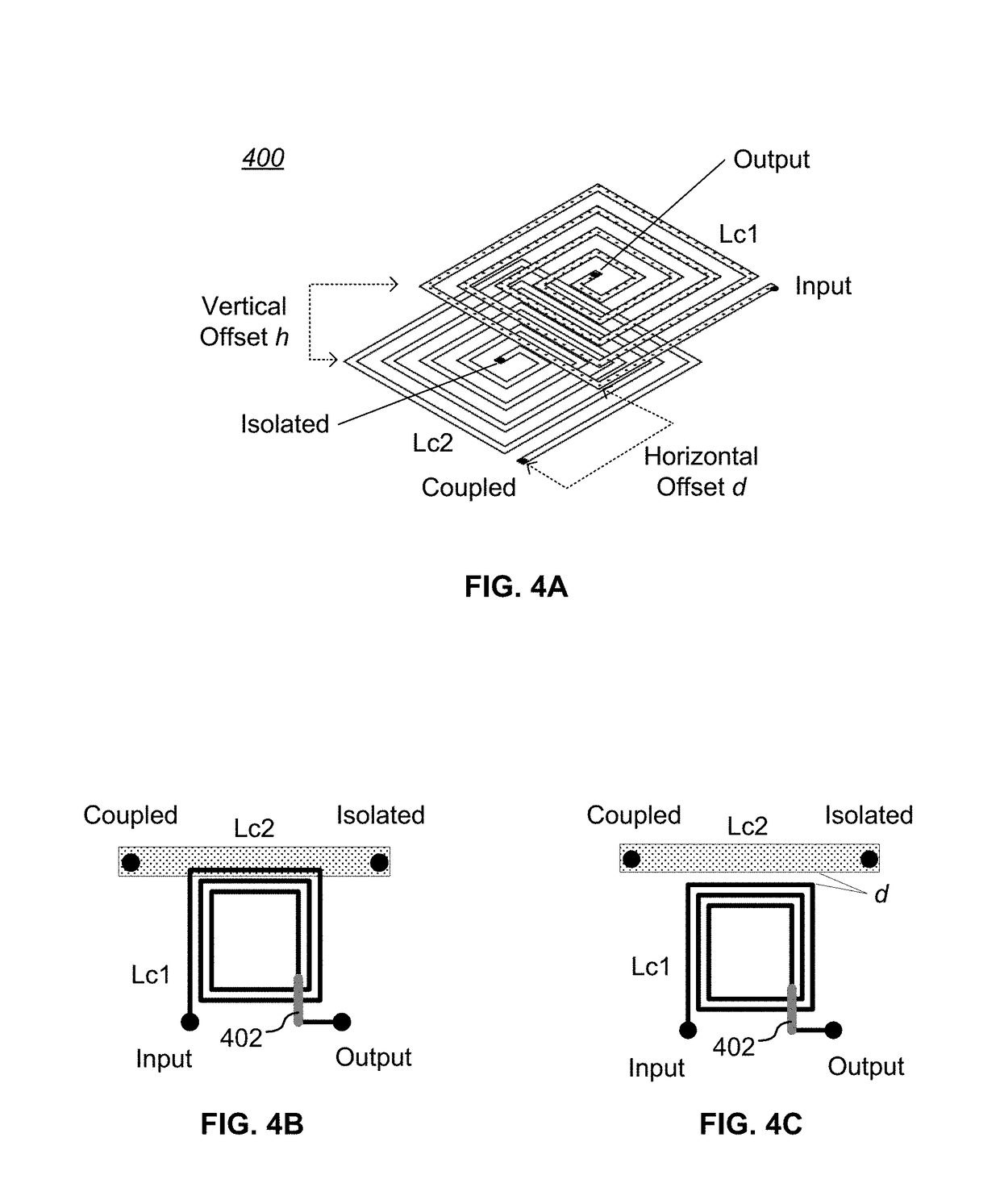
A ultra-compact coupler designed to sample the actual output power of a power amplifier and which is “VSWR insensitive”, such that reflected power is essentially not coupled to a detector circuit and only forward power is detected and processed. In a first embodiment, a coupler is situated between the final amplifier stage of a power amplifier and an output impedance matching network, and is specially configured for operation in a low impedance environment in conjunction with a detector circuit, thereby substantially reducing the areal size of the coupler. In a second embodiment, a coupler is integrated within an output impedance matching network coupled to the final amplifier stage of a power amplifier so as to share an inductor between the coupler and the output impedance matching network, thereby further substantially reducing the areal size of the coupler.

Description

CROSS-REFERENCE TO RELATED APPLICATIONS[0001]This invention may be related to U.S. patent application Ser. No. 15 / 594,336 (Attorney Docket No. PER-220-PAP), filed May 12, 2017, entitled “Compact Low Loss Signal Coupler”, assigned to the assignee of the present invention and hereby incorporated by reference.BACKGROUND(1) Technical Field[0002]This invention relates to electronic circuits, and more particularly to coupler circuits.(2) Background[0003]Power amplifiers (PAs) are used in a multitude of electronic systems, particularly radio frequency (RF) systems such as radios, cellular telephones, WiFi, etc. FIG. 1 is a block diagram of a prior art radio transmitter two-stage power amplifier 100. In the illustrated example, an integrated circuit (IC) 102 includes several subcircuits that accept an RF input signal RFIN and generate an amplified output signal RFOUT to a selected destination (e.g., one or more band filters, RF signal switches, and / or antennas); the IC 102 may also be refer...

Claims


Application Information

Patent Timeline
Patent Type & Authority Applications(United States)
IPC IPC(8): H03F1/30H03F3/195H03F3/213H03F1/56
CPCH03F1/30H03F3/195H03F3/213H03F1/56H03F2200/451H03F2200/222H03F2200/387H03F2200/465H03F2200/318H01P5/028H03F1/565H03F3/191
Inventor CHENG, CHIH-CHIEHRANTA, TERO TAPIO
Owner PSEMI CORP
Learn More