

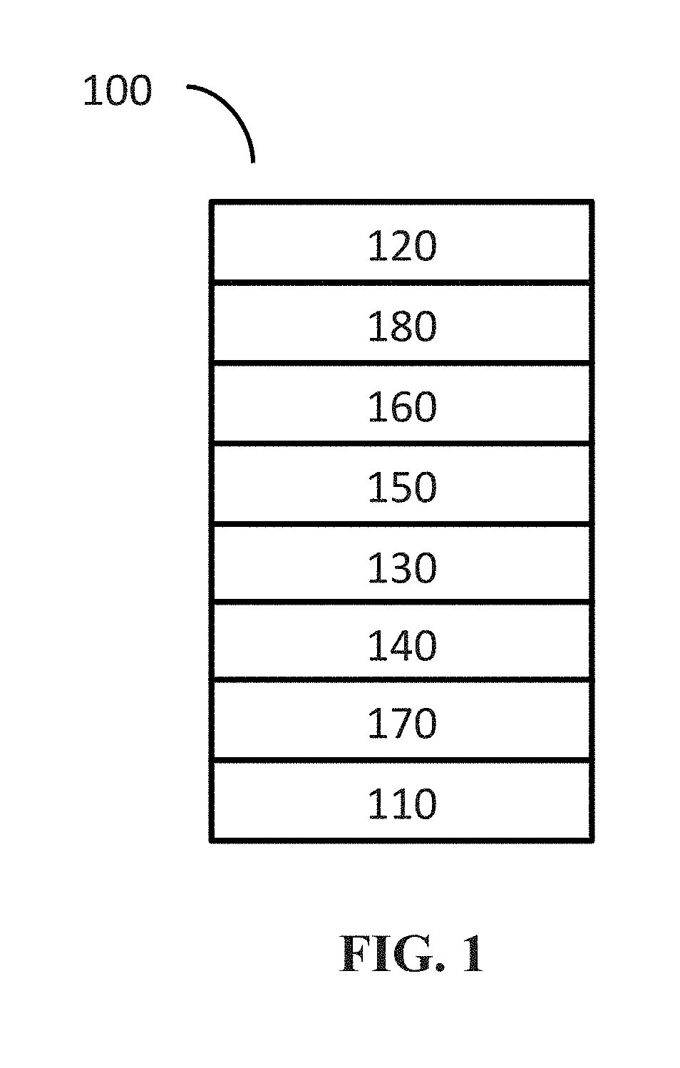
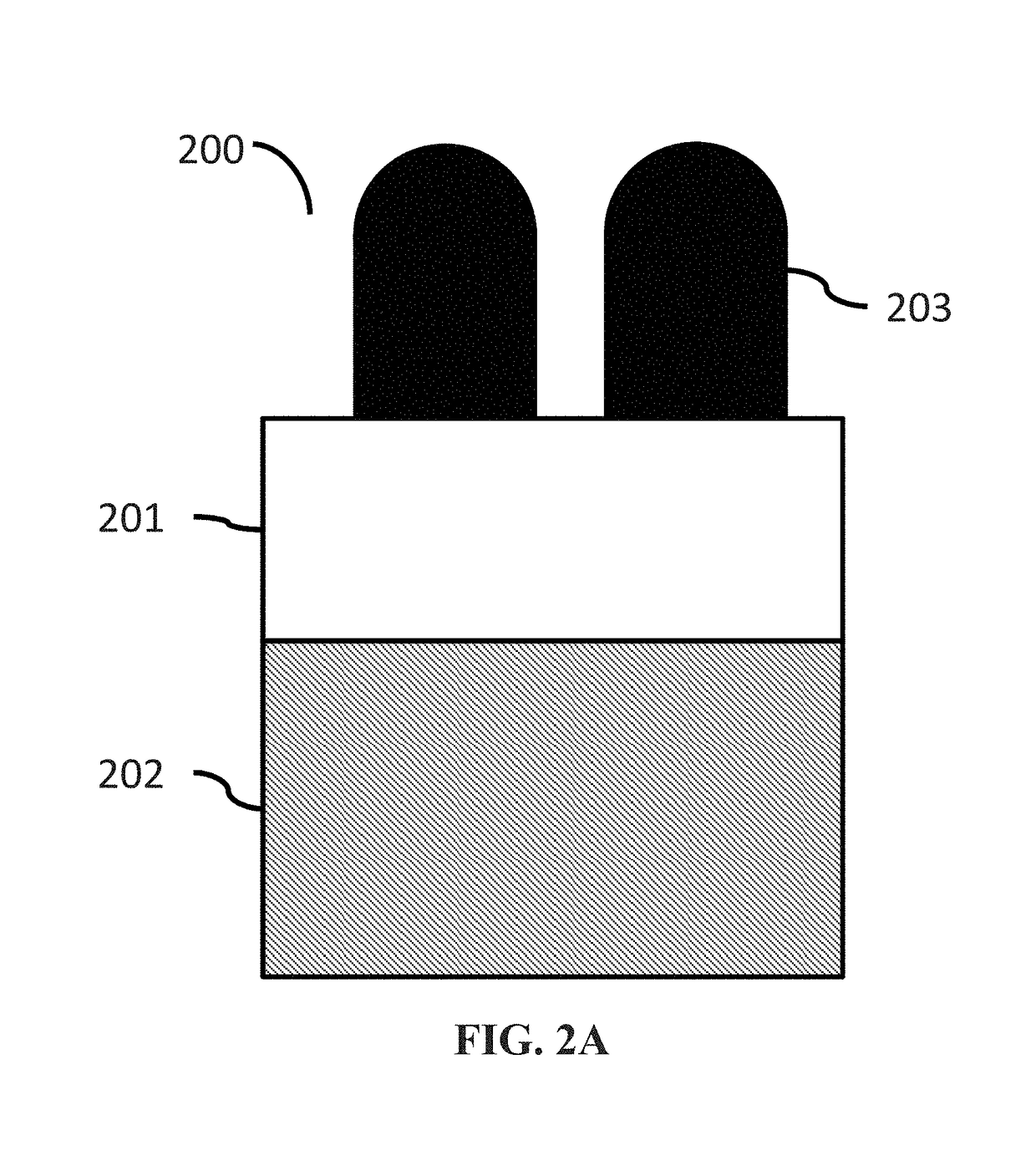
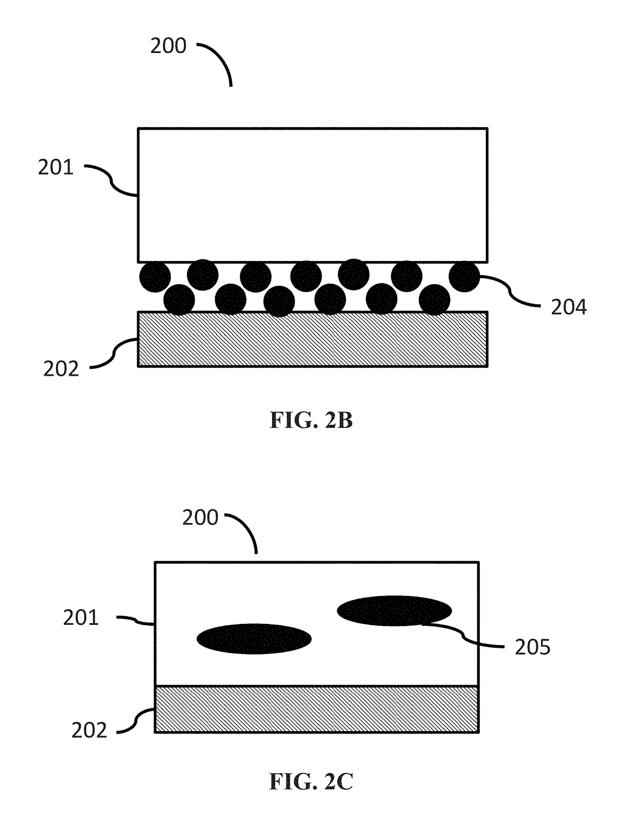
Phosphorescent emitters and extrinsic method for increasing stability thereof
a phosphorescent and extrinsic technology, applied in the direction of solid-state devices, semiconductor devices, organic semiconductor devices, etc., can solve the problems of no commercial oled lighting or display products incorporating high-efficiency blue phosphorescent or tadf emitters, inability to maintain both long-term stability and high efficiency, and achieve stable emission and stable triplet state of molecules
- Summary
- Abstract
- Description
- Claims
- Application Information
AI Technical Summary
Benefits of technology
Problems solved by technology
Method used
Image

Examples
Embodiment Construction
[0020]Before the present invention is described in further detail, it is to be understood that the invention is not limited to the particular embodiments described, as such may, of course, vary. It is also to be understood that the terminology used herein is for the purpose of describing particular embodiments only, and is not intended to be limiting, since the scope of the present invention will be limited only by the appended claims.
[0021]Where a range of values is provided, it is understood that each intervening value, to the tenth of the unit of the lower limit unless the context clearly dictates otherwise, between the upper and lower limit of that range and any other stated or intervening value in that stated range is encompassed within the invention. The upper and lower limits of these smaller ranges may independently be included in the smaller ranges is also encompassed within the invention, subject to any specifically excluded limit in the stated range. Where the stated rang...
PUM
| Property | Measurement | Unit |
|---|---|---|
| thickness | aaaaa | aaaaa |
| thickness | aaaaa | aaaaa |
| internal quantum efficiencies | aaaaa | aaaaa |
Abstract
Description
Claims
Application Information