VARYING ENERGY BARRIERS OF MAGNETIC TUNNEL JUNCTIONS (MTJs) IN DIFFERENT MAGNETO-RESISTIVE RANDOM ACCESS MEMORY (MRAM) ARRAYS IN A SEMICONDUCTOR DIE TO FACILITATE USE OF MRAM FOR DIFFERENT MEMORY APPLICATIONS

a technology of random access memory and magnetic tunnel junction, which is applied in the field of magnetic tunnel junctions (mtjs) employed in mram, can solve the problem of allowing the realization of desired performance differences

Inactive Publication Date: 2019-02-28
QUALCOMM INC
View PDF7 Cites 21 Cited by
  • Summary
  • Abstract
  • Description
  • Claims
  • Application Information

AI Technical Summary

Benefits of technology

[0010]In other aspects disclosed herein, MTJs having different energy barriers are fabricated in the same layer(s) of the semiconductor die to avoid having to provide additional layers in the semiconductor die for different MRAMs. In one example, to fabricate MTJs having different energy barriers in the same layer(s) of the semiconductor die, a fabrication process is employed that includes forming a first blocking layer over a second bottom via, which is in an interconnect layer of a semiconductor die. Once the second bottom via is covered by the first blocking layer, a first MTJ stack film is deposited over a first bottom via in the interconnect layer of the semiconductor die. A portion of the f...

Problems solved by technology

Different memory applications may require different tradeoffs between access times and data retention performance as an example, where using M...

Method used


Image

  • VARYING ENERGY BARRIERS OF MAGNETIC TUNNEL JUNCTIONS (MTJs) IN DIFFERENT MAGNETO-RESISTIVE RANDOM ACCESS MEMORY (MRAM) ARRAYS IN A SEMICONDUCTOR DIE TO FACILITATE USE OF MRAM FOR DIFFERENT MEMORY APPLICATIONS
  • VARYING ENERGY BARRIERS OF MAGNETIC TUNNEL JUNCTIONS (MTJs) IN DIFFERENT MAGNETO-RESISTIVE RANDOM ACCESS MEMORY (MRAM) ARRAYS IN A SEMICONDUCTOR DIE TO FACILITATE USE OF MRAM FOR DIFFERENT MEMORY APPLICATIONS
  • VARYING ENERGY BARRIERS OF MAGNETIC TUNNEL JUNCTIONS (MTJs) IN DIFFERENT MAGNETO-RESISTIVE RANDOM ACCESS MEMORY (MRAM) ARRAYS IN A SEMICONDUCTOR DIE TO FACILITATE USE OF MRAM FOR DIFFERENT MEMORY APPLICATIONS

Examples


Embodiment Construction

[0029]With reference now to the drawing figures, several exemplary aspects of the present disclosure are described. The word “exemplary” is used herein to mean “serving as an example, instance, or illustration.” Any aspect described herein as “exemplary” is not necessarily to be construed as preferred or advantageous over other aspects.

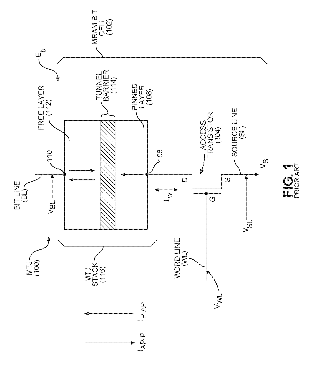
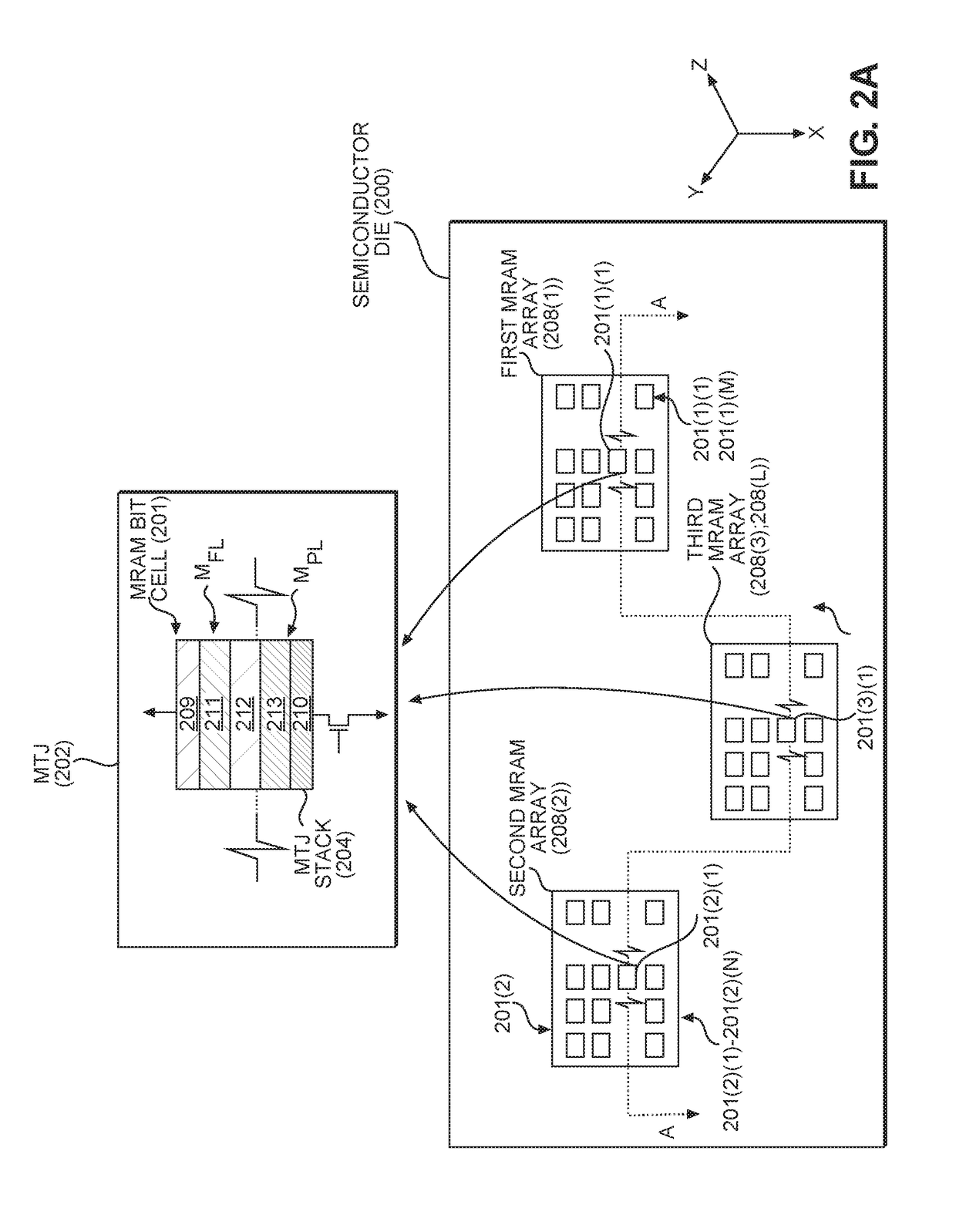
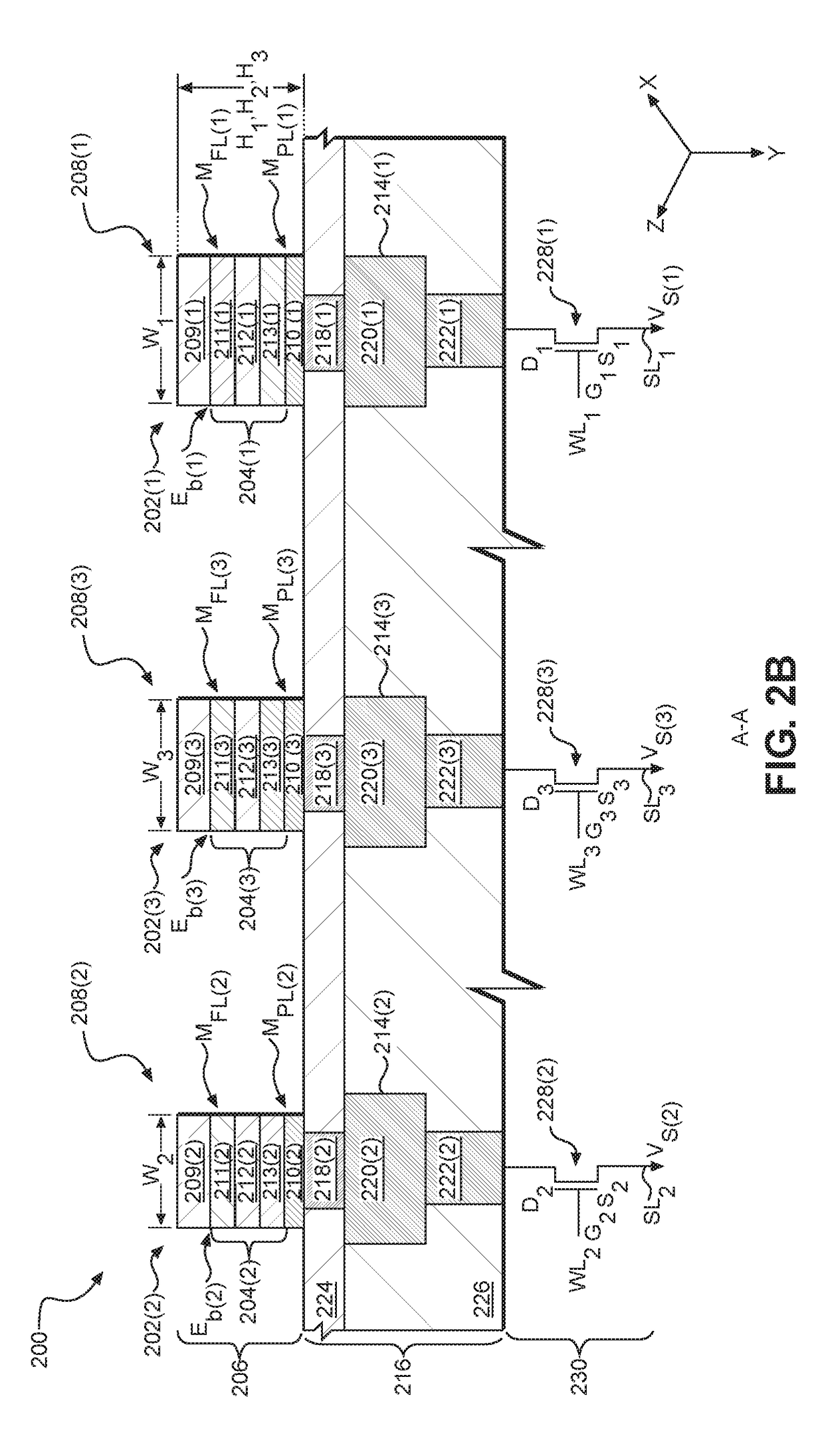
[0030]Aspects disclosed in the detailed description include varying energy barriers of magnetic tunnel junctions (MTJs) in different magneto-resistive random access memory (MRAM) arrays in a semiconductor die to facilitate use of MRAM for different memory applications. Different memory applications may require different tradeoffs between access times and data retention performance as an example, where using MTJ stacks having the same energy barrier in these different memory applications may not allow the desired differences in performance to be realized. Thus, in this regard, in exemplary aspects disclosed herein, to facilitate use of MRAM for differe...


PUM


Abstract

Varying energy barriers of magnetic tunnel junctions (MTJs) in different magneto-resistive random access memory (MRAM) arrays in a semiconductor die to facilitate use of MRAM for different memory applications is disclosed. In one aspect, energy barriers of MTJs in different MRAM arrays are varied. The energy barrier of an MTJ affects its write performance as the amount of switching current required to switch the magnetic orientation of a free layer of the MTJ is a function of its energy barrier. Thus, by varying the energy barriers of the MTJs in different MRAM arrays in a semiconductor die, different MRAM arrays may be used for different types of memory provided in the semiconductor die while still achieving distinct performance specifications. The energy barrier of an MTJ can be varied by varying the materials, heights, widths, and/or other characteristics of MTJ stacks.

Description

BACKGROUNDI. Field of the Disclosure[0001]The technology of the disclosure relates generally to magneto-resistive random access memory (MRAM), and more particularly to magnetic tunnel junctions (MTJs) employed in MRAM.II. Background[0002]Semiconductor storage devices are used in integrated circuits (ICs) in electronic devices to provide data storage. One example of a semiconductor storage device is magneto-resistive random access memory (MRAM). MRAM is non-volatile memory in which data is stored by programming a magnetic tunnel junction (MTJ) as part of an MRAM bit cell. One advantage of MRAM is that MTJs in MRAM bit cells can retain stored information even when power is turned off. This is because data is stored in the MTJ as a small magnetic element rather than as an electric charge or current.[0003]In this regard, an MTJ comprises a free ferromagnetic layer (“free layer”) disposed above or below a fixed or pinned ferromagnetic layer (“pinned layer”). The free and pinned layers ar...

Claims


Application Information

Patent Timeline
IPC IPC(8): G11C11/16H01F10/32G11C11/15H01L43/08
CPCG11C11/161G11C11/1653H01F10/3295H01L43/08G11C11/1659G11C11/1675G11C11/15H10B61/22H10N50/01H10N50/10
Inventor LI, XIACHEN, WEI-CHUANHSU, WAH NAMKANG, SEUNG HYUK
Owner QUALCOMM INC
Why Eureka
Try Eureka